Plane display with VMOS cathode structure and manufacturing technology

A cathode structure and display technology, applied in cold cathode manufacturing, electrode system manufacturing, discharge tube/lamp manufacturing, etc., can solve the problems of affecting the voltage, poor adhesion, and carbon nanotubes falling off, etc., to reduce Production cost, the effect that is conducive to mass production

Inactive Publication Date: 2006-05-24
ZHONGYUAN ENGINEERING COLLEGE
View PDF0 Cites 9 Cited by
  • Summary
  • Abstract
  • Description
  • Claims
  • Application Information

AI Technical Summary

Problems solved by technology

From the perspective of preparation methods, most of them use the transplantation method. In the process of transplantation, affected by various factors such as production process, baking process, and slurry production, the ability of field emission electrons has been reduced. From the perspective of cathode resistance, due to the need to make an additional cathode electrode layer under the carbon nanotube cathode, in order to ensure that the external voltage can be successfully applied to the carbon nanotube cathode, however, the resistance in the cathode electrode layer The change of the resistance value greatly affects the voltage applied to the carbon nanotubes; from the point of view of the adhesion of the carbon nanotube cathode, this is also a problem worthy of attention. If the carbon nanotube cathode and the bottom substrate If the adhesion between them is not very good, then when the electric field is strengthened, the carbon nanotubes are extremely easy to fall off from the substrate, causing permanent damage to the display device; etc., how to take practical and effective measures, can It is a practical problem that researchers have seriously considered to allow large-area carbon nanotube cathodes to achieve uniform and stable emission of a large number of electrons.

Method used


Image

  • Plane display with VMOS cathode structure and manufacturing technology
  • Plane display with VMOS cathode structure and manufacturing technology
  • Plane display with VMOS cathode structure and manufacturing technology

Examples


Embodiment Construction

[0055] The present invention will be further described below in conjunction with the accompanying drawings and embodiments, but the present invention is not limited to these embodiments.

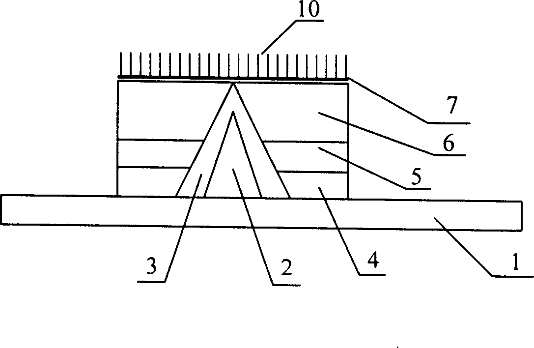
[0056] The VMOS cathode structure in the present invention includes cathode glass panel 1, metal layer 2, insulating layer 3, n-type heavily doped silicon layer [4], p-type doped silicon layer [5], n-type doped silicon layer [6] ], cathode electrode layer [7], and use the following process to make:

[0057] 1. Fabrication of cathode glass panel [1]

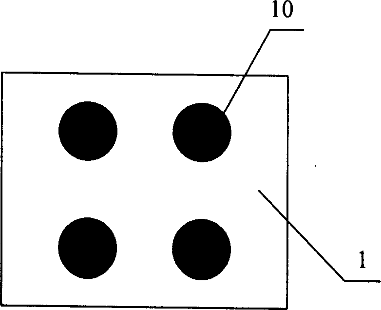
[0058] Cut the whole flat soda-lime glass to make the cathode glass panel[1];

[0059] 2. Fabrication of the metal layer [2]

[0060] Prepare a chromium layer on the cathode glass panel; combine the conventional photolithography process to etch the chromium layer to form a metal layer [2]; the middle part of the etched chromium layer is required to form an inverted "V" shape structure, with the tip pointing away from the cathode glass panel; ...


PUM


Abstract

The disclosed display includes following components: sealed vacuum cavity composed of cathode glass faceplate, anode glass faceplate, and around glass surrounded frame; anode pole layer on the anode glass faceplate, and phosphor powder layer printed on anode pole layer; control grid in use for controlling electron emission of carbon Nano tube; cathode of carbon Nano tube and VMOS cathode structure printed on cathode glass faceplate; back wall structure and accessory element of getter. VMOS cathode structure is in use for adjusting current value in cathode pole layer, and further for adjusting voltage on cathode of carbon Nano tube in order to guarantee that carbon Nano tube can transmit a mass of electrons uniformly and stably. Advantages are: stable and reliable preparing procedure, simple technique, low cost, and simple structure.

Description

technical field [0001] The invention belongs to the fields of plane display technology, microelectronic science and technology, vacuum science and technology, and nano science and technology, and relates to the manufacture of flat panel field emission displays, in particular to flat panels for carbon nanotube cathodes. The content of device fabrication of field emission display, especially related to the fabrication process of field emission flat display device with VMOS cathode structure and carbon nanotube cathode. Background technique [0002] Carbon nanotubes have a unique geometric shape, small tip curvature radius, and extremely high mechanical strength. Under the action of an external electric field, they can emit a large number of electrons. They are an ideal cold cathode material. For field emission flat panel display devices using carbon nanotubes as cathode materials, image quality is one of the key technical indicators to measure the success of device fabrication...

Claims


Application Information

Patent Timeline
Patent Type & Authority Applications(China)
IPC IPC(8): H01J31/12H01J1/304H01J9/02H01J29/04
Inventor 李玉魁
Owner ZHONGYUAN ENGINEERING COLLEGE
Why Eureka
Try Eureka