Method of producing laser-processed product and adhesive sheet, for laser processing used therefor

A technology of laser processing and manufacturing method, which is applied in manufacturing tools, film/sheet adhesives, semiconductor/solid-state device manufacturing, etc. The effect of precision and reliability

Inactive Publication Date: 2006-05-31
NITTO DENKO CORP
View PDF3 Cites 14 Cited by
  • Summary
  • Abstract
  • Description
  • Claims
  • Application Information

AI Technical Summary

Problems solved by technology

Therefore, the manufacturing efficiency of semiconductor chips deteriorates

Method used


Image

  • Method of producing laser-processed product and adhesive sheet, for laser processing used therefor
  • Method of producing laser-processed product and adhesive sheet, for laser processing used therefor
  • Method of producing laser-processed product and adhesive sheet, for laser processing used therefor

Examples


no. 1 Embodiment approach

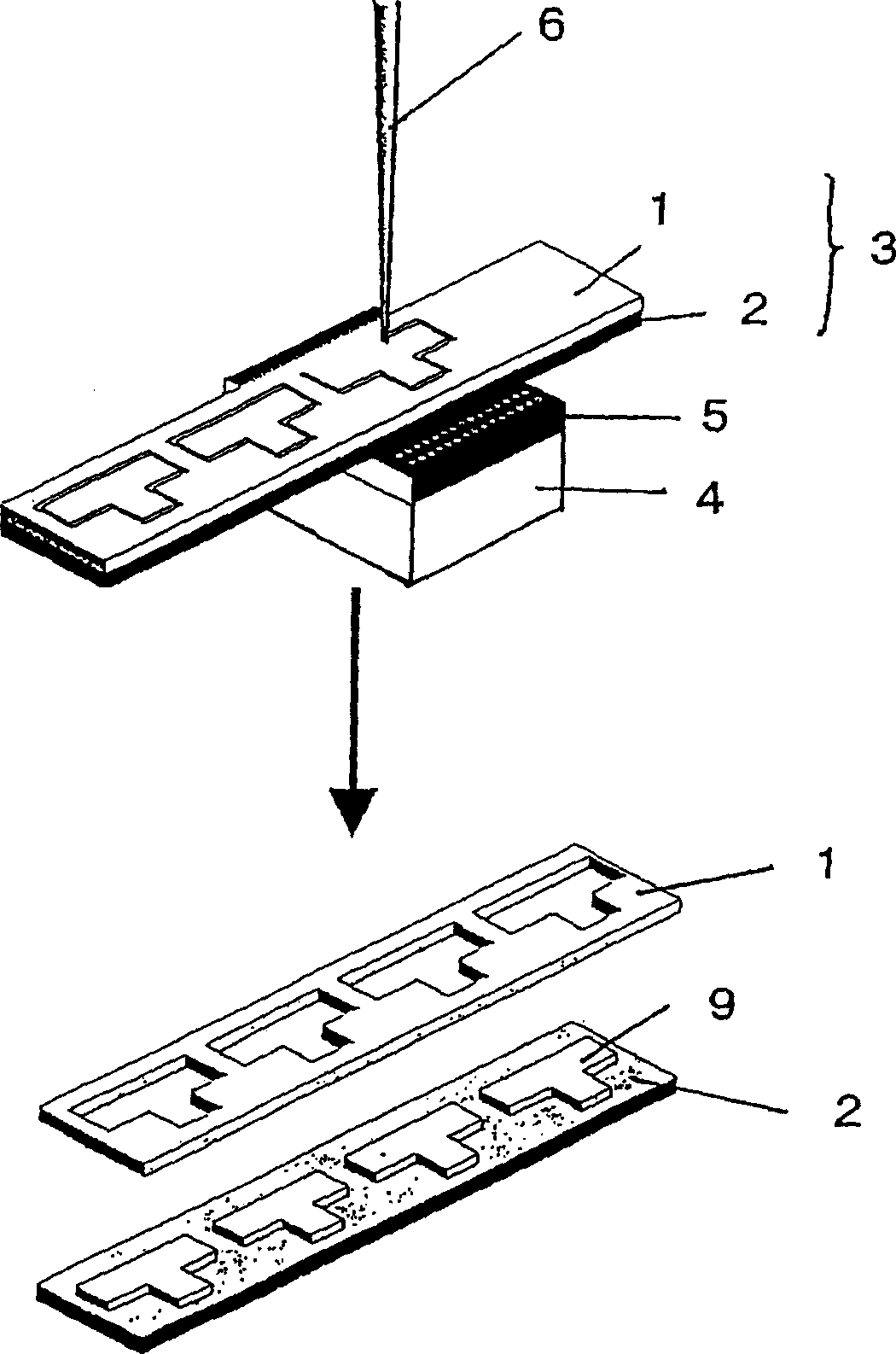
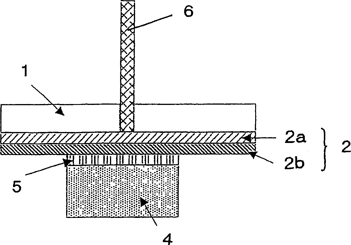
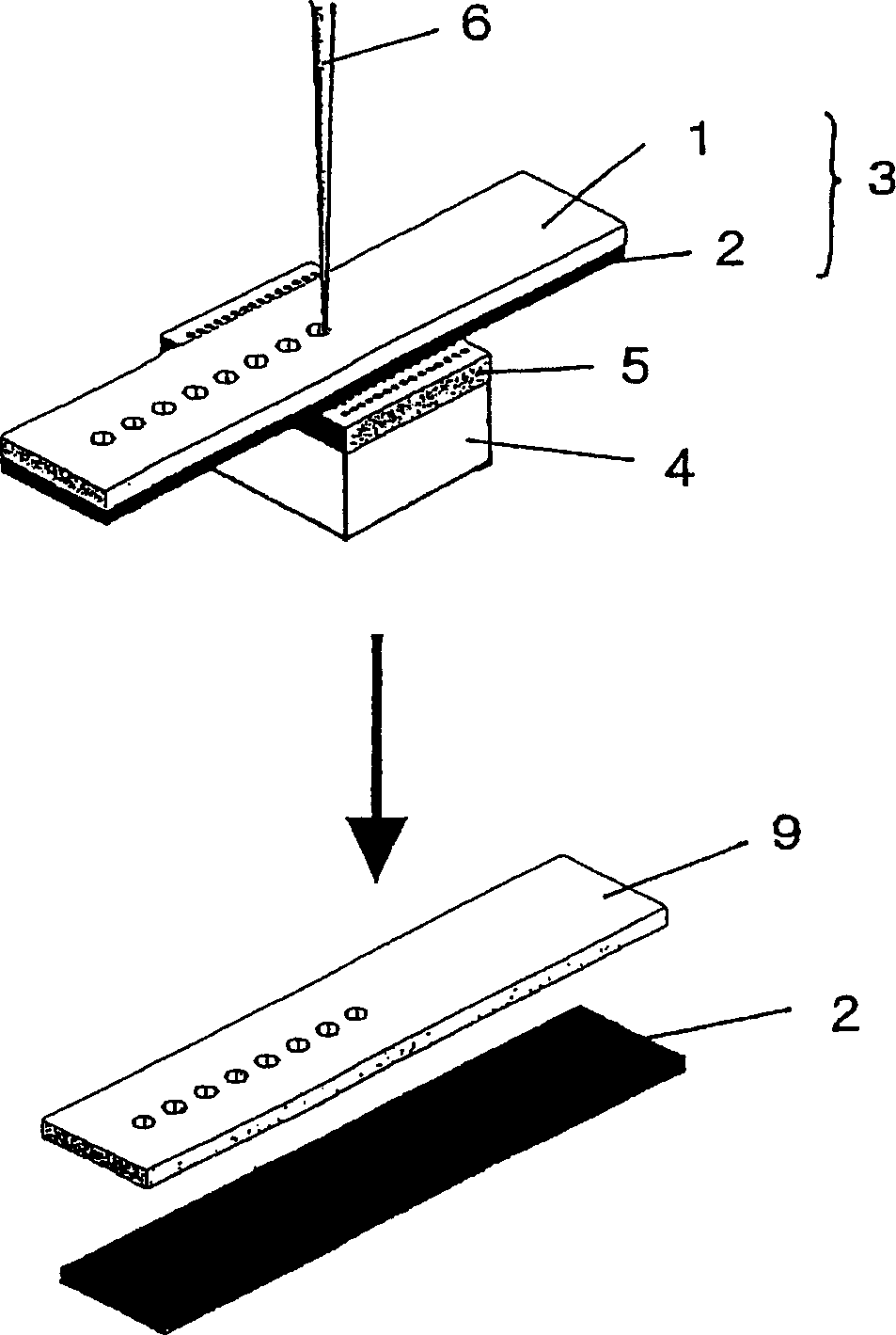
[0107] [adhesive sheet]

[0108] First, the PSA sheet used in the first embodiment of the present invention will be described. The pressure-sensitive adhesive sheet in this embodiment is used when processing a workpiece by ablation using laser light having a wavelength in the ultraviolet region or laser light capable of absorbing light in the ultraviolet region through a multiphoton absorption process. Its structure is that at least an adhesive layer is provided on a substrate (details of the substrate and the adhesive layer will be described later). As the PSA sheet used in this embodiment, there are eight types of PSA sheets A to H described below in more detail.

[0109] (adhesive sheet A)

[0110] The pressure-sensitive adhesive sheet A has physical properties such that the ratio of the light absorption coefficient obtained in the following formula (1) is less than 1 when irradiated with laser light whose intensity causes ablation of the workpiece The irradiation intens...

no. 2 Embodiment approach

[0195] The second embodiment relates to a method of performing laser processing on a workpiece made of a metal-based material in particular.

[0196] [adhesive sheet]

[0197] As the PSA sheet used in this embodiment, there are six types of PSA sheets A' to F' described below. Note that detailed descriptions of components having the same functions as those of the various pressure-sensitive adhesive sheets of the first embodiment described above are omitted.

[0198] (adhesive sheet A')

[0199] Compared with the above-mentioned adhesive sheet A, the adhesive sheet A' has an absorption coefficient of less than 20 cm at a relative wavelength of 355 nm laser light. -1 This is different.

[0200] In the case where the workpiece is made of a metal-based material, when the PSA sheet A' in this embodiment shows a light of less than 20 cm at 355 nm light, -1 When the light absorption coefficient of , it is shown that the adhesive sheet A' is more difficult to process than the proc...

Embodiment 1

[0229] The following examples and the like correspond to the above-mentioned adhesive sheets A and A'.


PUM

PropertyMeasurementUnit
densityaaaaaaaaaa
tensile strengthaaaaaaaaaa
absorption coefficientaaaaaaaaaa

Abstract

PROBLEM TO BE SOLVED: To provide a method for subjecting works, such as, for example, various kinds of sheet materials, circuit boards, semiconductor wafers, glass substrates, ceramic substrates, metallic substrates, light emitting or light receiving element substrates for semiconductor lasers etc., MEMS substrates, semiconductor packages, cloth, leather, and paper, to working such as, for example, cutting and perforating. SOLUTION: The method of working the works by using UV absorption abrasion of a laser includes (1) a process of sticking a tacky adhesive sheet of ≥50% in transmittance in an absorption region of a laser beam to a surface of the work opposite to the surface to be irradiated with the laser, (2) a process of working the work by irradiating the work with the laser, and (3) a process of peeling off the tacky adhesive sheet. COPYRIGHT: (C)2005,JPO&NCIPI

Description

technical field [0001] The present invention relates to a method of using a laser to treat light-emitting or light-receiving element substrates, MEMS substrates, semiconductor packages (packages), cloth, Manufacturing method of laser workpieces such as cutting, punching, marking, grooving, scribing, or edge trimming of processed objects such as leather and paper, and adhesive sheets for laser processing used in the method . Background technique [0002] Along with the miniaturization of electrical and electronic equipment in recent years, the miniaturization and high-precision of components are progressing, and the contour processing of various materials is also pursuing high-precision and high-precision processing with a machining accuracy of ±50 μm or less. . However, conventional punching such as punching has an accuracy of about ±100 μm at best, which cannot meet such demands. In addition, high-precision and high-precision drilling of various materials is also require...

Claims


Application Information

Patent Timeline
Patent Type & Authority Applications(China)
IPC IPC(8): B23K26/00B23K26/18B23K26/16C09J7/02H01L21/301H05K3/00
Inventor 浦入正胜日野敦司松尾直之高桥智一松村健山本昌司
Owner NITTO DENKO CORP
Why Eureka
Try Eureka