
Method for making three-electrode flat-type display based on carbon nano-tube field emission array

The technology of a carbon nanotube and a manufacturing method is applied in the field of manufacturing a three-electrode flat display based on a carbon nanotube field emission array, and can solve the problems of high cost, low electron transmission efficiency, and difficulty in gate manufacturing.

Inactive Publication Date: 2006-06-21
XI'AN INST OF OPTICS & FINE MECHANICS - CHINESE ACAD OF SCI
View PDF0 Cites 3 Cited by
  • Summary
  • Abstract
  • Description
  • Claims
  • Application Information

AI Technical Summary

Problems solved by technology

[0003] The purpose of the present invention is to provide a method for manufacturing a three-electrode planar display based on a carbon nanotube field emission array, which solves the technical problems of high difficulty in gate fabrication, low electron transmission efficiency, and high cost in the background art

Method used


Image

  • Method for making three-electrode flat-type display based on carbon nano-tube field emission array
  • Method for making three-electrode flat-type display based on carbon nano-tube field emission array
  • Method for making three-electrode flat-type display based on carbon nano-tube field emission array

Examples


Embodiment Construction

[0129] 1. Fabrication of glass grooves

[0130] The glass groove is directly formed on the rear substrate by physical or chemical etching. The process includes the formation of the template, uniform glue, exposure, sol, etching and other processes. It can also be printed by screen printing with glass glue Technology formation can also be formed by "sandblasting" with ion beams. The depth and width of glass grooves are generally around tens of microns to 100 microns, which are limited by process conditions and device spatial resolution.

[0131] 2. Preparation of carbon nanotube slurry

[0132] 1] Preparation and purification of carbon nanotubes. Regardless of whether it is single-walled or double-walled carbon nanotubes, the preparation and purification technologies are relatively mature. Among them, the preparation technologies include chemical vapor deposition, arc discharge, hot wire plasma, and laser ablation. It should be pointed out that What is more interesting is tha...


PUM


Abstract

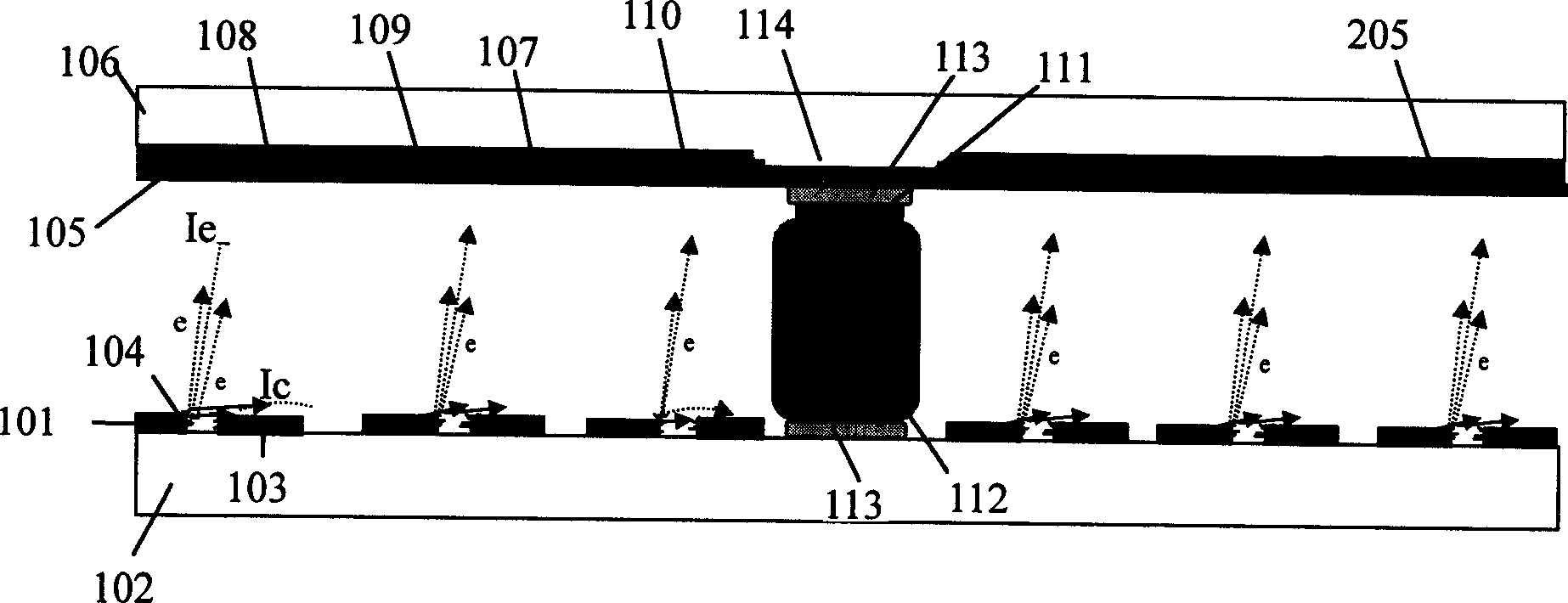
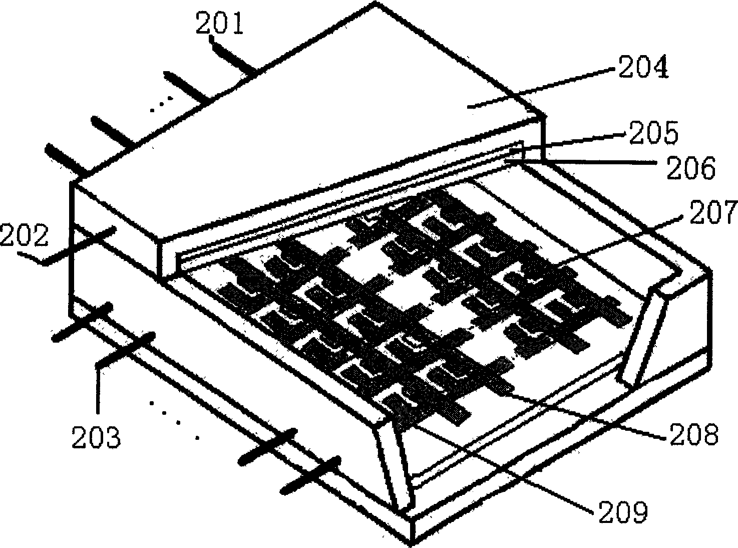
The manufacture method for three-electrode plane display unit based on nano carbon tube field-emission array comprises: 1) preparing cathode, grid and routing electrode on post substrate; 2) preparing nano carbon tube array on cathode; 3) preparing phosphor screen and anode on front substrate; 4) manufacturing separant between the front and post substrates; 5) packaging the display unit. This invention combines plane emission structure and strong emission property of nano carbon tube, overcomes problems in prior art, and has high electron transport rate (40% in theoretical calculation and 29.3% in experiment result), low cost, and convenient to regulation.

Description

technical field [0001] The invention relates to a manufacturing method of a flat display, in particular to a manufacturing method of a field emission flat display. Background technique [0002] Field Emission Display (Field Emission Display-FED) is considered to be the best successor of CRT, which has the advantages of both CRT and LCD, namely: (1) cold cathode emission; (2) low operating voltage, low power consumption; ( 3) Self-illumination and high brightness; (4) Wide viewing angle (170°); (5) High response speed (microsecond level); (6) Wide range of ambient temperature changes; (7) No image distortion; (8) ) is not affected by the earth's magnetic field and other surrounding magnetic fields. Therefore, FED is considered to be the most ideal flat panel display device and one of the most important displays to be developed in the 21st century, with a broad market and good application prospects. The biggest advantage of FED is that it is a display with high brightness an...

Claims


Application Information

Patent Timeline
IPC IPC(8): H01J9/02H01J1/30H01J9/00H01J9/26H01J29/02H01J31/12
Inventor 田进寿白永林刘百玉欧阳娴赵宝升白晓红王琛黄蕾
Owner XI'AN INST OF OPTICS & FINE MECHANICS - CHINESE ACAD OF SCI
Learn More