Plasma etching method of reducing generation of fine dust

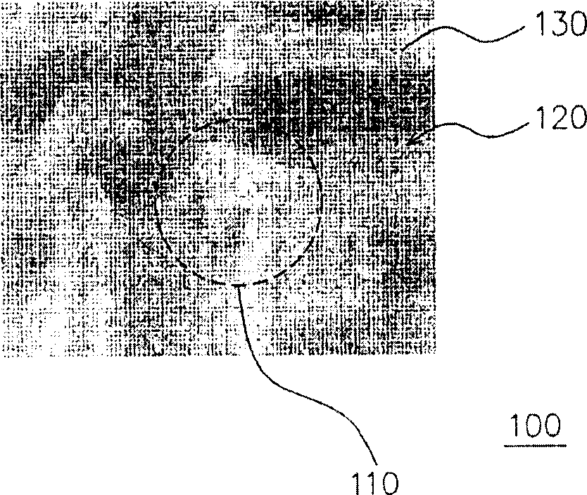
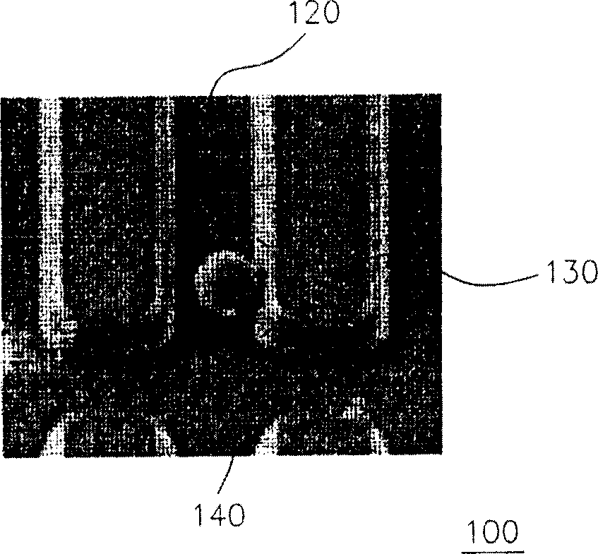
A plasma etching, oxygen plasma technology, applied in the direction of electrical components, semiconductor/solid-state device manufacturing, circuits, etc., can solve problems such as affecting the conduction properties of the circuit 130, and achieve the effect of avoiding the generation of dust and defects

Inactive Publication Date: 2006-07-05
UNITED MICROELECTRONICS CORP
View PDF0 Cites 6 Cited by
  • Summary
  • Abstract
  • Description
  • Claims
  • Application Information

AI Technical Summary

Problems solved by technology

However, if Figure 1B As shown, ball type defects (ball type defect) 140 will still be found on the fabricated trench 120, thereby affecting the conduction properties of the circuit 130.

Method used


Image

  • Plasma etching method of reducing generation of fine dust
  • Plasma etching method of reducing generation of fine dust
  • Plasma etching method of reducing generation of fine dust

Examples


Embodiment Construction

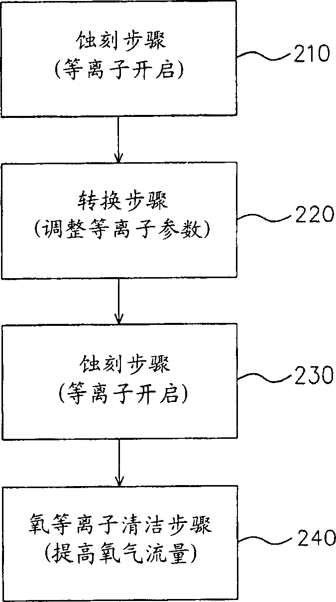
[0021] figure 2 What is shown is a schematic flow chart of a plasma etching method for reducing dust generation according to a preferred embodiment of the present invention. Please refer to figure 2 , The plasma etching method for reducing dust generation of the present invention at least includes an etching step 210 , a conversion step 220 , an etching step 230 and an oxygen plasma cleaning step 240 . Firstly, an etching step 210 is performed using an appropriate etching condition to etch the substrate. Then, before proceeding to the next etching step 230, a transition step 220 is performed. In this transition step 220, the plasma does not need to be turned off, so the temperature of the reaction chamber does not cool down. Then, after the etching step 230, an oxygen plasma cleaning step 240 is performed to remove plasma etching residues.

[0022] Such as figure 2 As shown, both the etching step 210 and the etching step 230 use plasma ionized gas to etch the substrate ...


PUM


Abstract

Being suitable for forming trench in substrate, the method includes steps: carrying out first etching step for the substrate under first etching condition; carrying out second etching step for the substrate under second etching condition; carrying out a conversion step between the first etching step and second etching step in order to adjust one of environmental parameters such as pressure condition in reaction chamber, gas flow, source power of plasma or temperature of reaction chamber; moreover, making variance of environmental parameters between etching step and conversion step be les than 15úÑ in order to maintain stabilized environment for reaction, and to avoid dropping off fine dust. Afterwards, when cleaning step of oxygen plasma is carried out, pressure in reaction chamber is raised to 40mTorr -80mTorr so as to prevent generation of spheroidal defect.

Description

technical field [0001] The invention relates to a plasma etching method, in particular to a plasma etching method which reduces dust generation and is suitable for making a shallow trench isolation structure (Shallow Trench Isolation, STI). Background technique [0002] In the semiconductor process, etching is mainly used for pattern transfer application. The general practice is to cooperate with the lithography process (lithography). First, a layer of photoresist is coated on the substrate, and then the pattern on the mask is patterned on the photoresist by an exposure process, and then the unexposed photoresist is removed with a developer , the patterned photoresist is then used as an etching mask, and an appropriate wet or dry etching technique is selected to remove part of the substrate, and finally the patterned photoresist is removed, and the The pattern on the mask is transferred to the substrate. [0003] The etching process in the semiconductor process mainly ado...

Claims


Application Information

Patent Timeline
Patent Type & Authority Applications(China)
IPC IPC(8): H01L21/3065H01L21/76
Inventor 简俊贤陈重吉
Owner UNITED MICROELECTRONICS CORP
Why Eureka
Try Eureka