Check patentability & draft patents in minutes with Patsnap Eureka AI!

Substrate processing apparatus and substrate processing method

A substrate processing device and substrate technology, applied in the direction of ion implantation plating, gaseous chemical plating, coating, etc., can solve the problem of smaller wiring and electrode processing size, inability to process multiple batches of substrate plasma, high frequency electric field, etc. problem, to achieve the effect of stable resistivity value and stable plasma treatment

Inactive Publication Date: 2006-08-30
TOKYO ELECTRON LTD
View PDF1 Cites 6 Cited by
  • Summary
  • Abstract
  • Description
  • Claims
  • Application Information

AI Technical Summary

Problems solved by technology

[0006] During the plasma processing of multiple batches of substrates, if the resistivity value of the focus ring changes, the distribution of the high-frequency electric field near the substrate changes, and there is a problem that stable plasma processing cannot be performed on multiple batches of substrates.
In particular, in recent years, the processing size of wiring and electrodes in semiconductor devices manufactured with substrates has been required to be reduced. Due to the requirement for the stability of the plasma atmosphere in the chamber, the requirements for the stability of the high-frequency electric field are higher than now. So it is possible to further surface the above problem

Method used


Image

  • Substrate processing apparatus and substrate processing method
  • Substrate processing apparatus and substrate processing method
  • Substrate processing apparatus and substrate processing method

Examples


Embodiment Construction

[0031] Embodiments of the present invention will be described below with reference to the drawings.

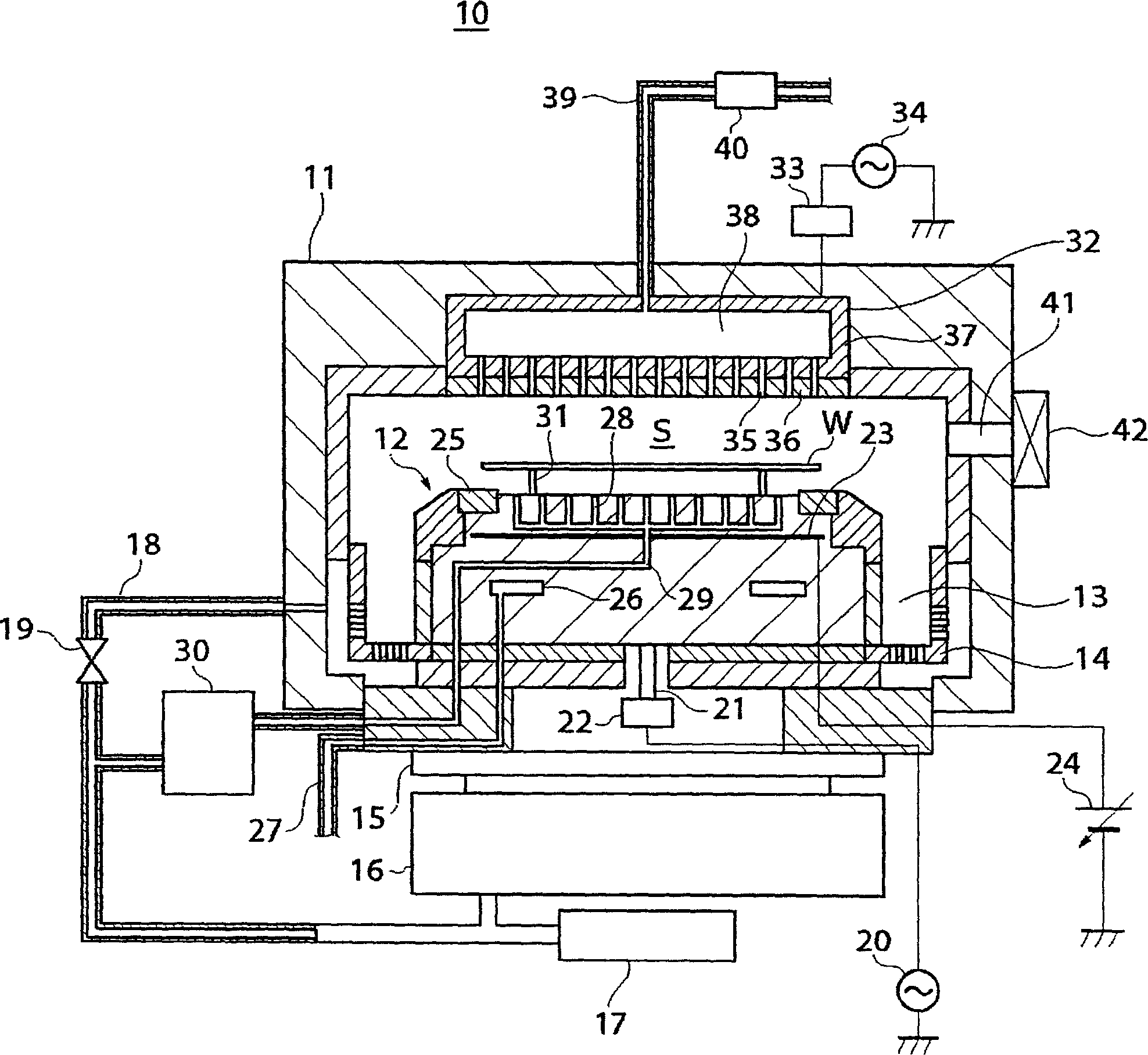
[0032] figure 1It is a cross-sectional view showing a schematic configuration of a substrate processing apparatus in an embodiment of the present invention.

[0033] exist figure 1 The middle substrate processing apparatus 10 performs dry etching (Reactive Ion Etching) (hereinafter referred to as “RIE”) as a desired plasma treatment on a semiconductor device wafer (hereinafter simply referred to as “wafer”) W, and has, for example, aluminum or stainless steel. A metal cylindrical chamber 11 is arranged inside the chamber 11 with a cylindrical susceptor 12 serving as a stage on which a wafer W having a diameter of 300 mm, for example, is placed.

[0034] In the substrate processing apparatus 10, the side wall of the chamber 11 and the side surface of the susceptor 12 are used to form an exhaust passage 13, and the exhaust passage 13 functions as a flow path for exhausting gas...


PUM


Abstract

A substrate processing apparatus that enables a plurality of substrates to be subjected to stable plasma processing. A chamber 11 houses a wafer W. The wafer W is subjected to reactive ion etching (RIE) in the chamber 11. A focus ring 25 has P-type silicon as a parent material thereof. At least part of the focus ring 25 is exposed to an interior of the chamber 11. The focus ring 25 has been subjected to heat treatment at least once.

Description

technical field [0001] The present invention relates to a substrate processing apparatus and a substrate processing method, and more particularly to a substrate processing apparatus having constituent members having p-type silicon as a base material arranged in a processing chamber where plasma is generated. Background technique [0002] Generally, a substrate processing apparatus for performing predetermined plasma processing on a substrate such as a wafer for a semiconductor device has a processing chamber (hereinafter referred to as a "chamber") for accommodating a substrate and performing plasma processing. In this substrate processing apparatus, a processing gas is introduced into a chamber, and a high-frequency electric field is generated in the chamber to convert the processing gas into plasma to generate ions and radicals, and plasma processing is performed on a substrate using the ions and radicals. [0003] In the chamber, a focus ring made of silicon is disposed a...

Claims


Application Information

Patent Timeline
IPC IPC(8): H01L21/00H01L21/20H01L21/3065H01L21/67C23C16/44C23C14/22C23F4/00H05H1/00H01J37/32
Inventor 宫野真一
Owner TOKYO ELECTRON LTD
Features
  • R&D
  • Intellectual Property
  • Life Sciences
  • Materials
  • Tech Scout
  • Unparalleled Data Quality
  • Higher Quality Content
  • 60% Fewer Hallucinations
Learn More