Semiconductor luminescent element composition

A technology of light-emitting elements and semiconductors, which is applied in the direction of semiconductor devices, electrical components, and electric solid-state devices, and can solve problems such as low acceptance, high prices, and reduced product reliability.

Active Publication Date: 2006-08-30
EPISTAR CORP
View PDF1 Cites 19 Cited by
  • Summary
  • Abstract
  • Description
  • Claims
  • Application Information

AI Technical Summary

Problems solved by technology

Therefore, due to the difference in coefficient of thermal expansion, it is very easy to cause various phenomena such as bending and fatigue between the light emitting diode (12) and the heat sink (10) due to high temperature during use or process, and greatly reduce the reliability of the product (reliability)
In order to shorten the difference in thermal expansion coefficients between materials, ceramic materials with low thermal expansion coefficients are also used in the prior art, such as aluminum nitride (AlN). However, ceramic materials such as aluminum nitride are too expensive and are not accepted by the market. high

Method used


Image

  • Semiconductor luminescent element composition
  • Semiconductor luminescent element composition
  • Semiconductor luminescent element composition

Examples


no. 1 example

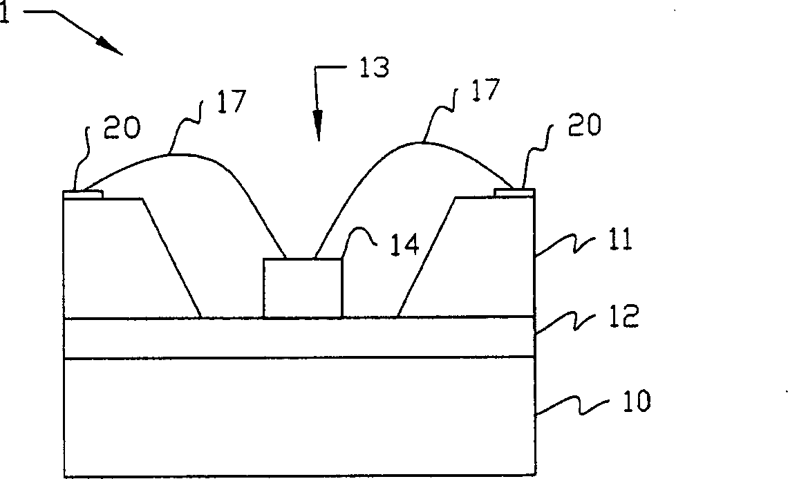
[0029] Figure 1a and 1b A structural diagram showing a semiconductor light emitting element composition 1 according to an embodiment of the present invention. The meanings of each mark are as follows, 1 indicates the composition of the semiconductor light-emitting element; 10 indicates the composite material substrate; 11 indicates the circuit layout carrier; 12 indicates the bonding structure; 13 indicates the recessed space; 14 indicates the semiconductor light-emitting element; 17 indicates the wire; 20 Indicates an electrical contact. In addition, the same elements in the following other drawings will be marked with the same symbols, and will not be repeated, and will be described first.

[0030] Firstly, after the recessed space 13 is formed on the circuit layout carrier 11 , the circuit layout carrier 11 and the composite material substrate 10 are combined with the bonding structure 12 . Next, the semiconductor light emitting element 14 is fixed in the recessed space ...

no. 2 example

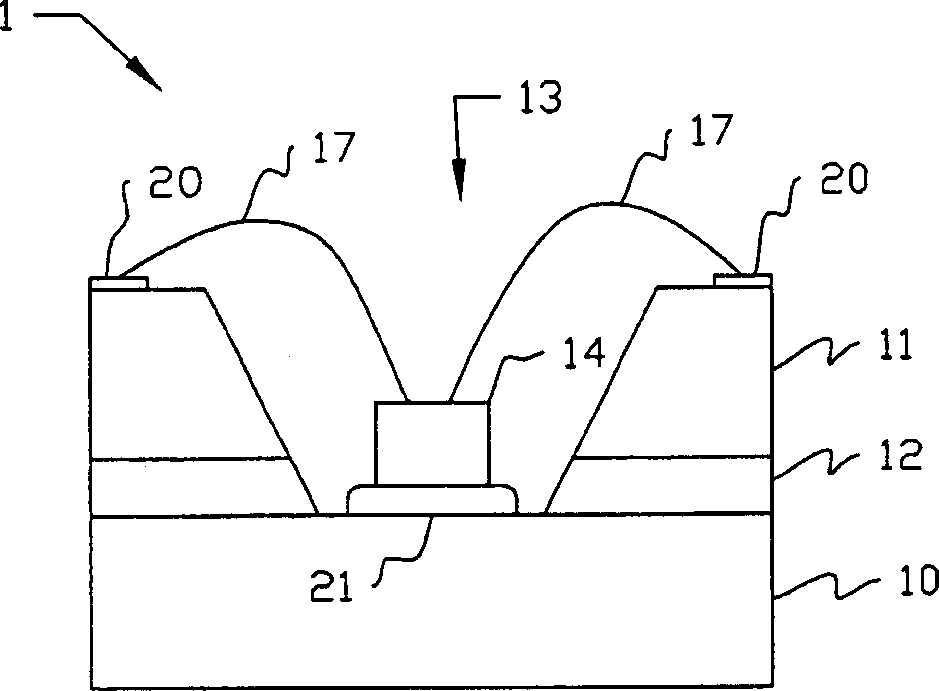
[0039] figure 2 A structural diagram showing a semiconductor light emitting element composition 1 according to another embodiment of the present invention. Wherein, mark 1201 represents a soft viscous material layer; 1202 and 1203 represent a reaction layer; 15 represents a reflection layer; 16 represents a planarization layer;

[0040] As described in the first embodiment, the semiconductor light emitting element 14 of the present invention is combined with the circuit layout carrier 11 via the adhesive structure 12 . In addition, in addition to using the above-mentioned soft adhesive material, other materials can be used in combination to further improve the adhesive properties of the adhesive structure 12 . Such as figure 2 As shown, the adhesive structure 12 includes a soft adhesive material layer 1201 , and reactive layers 1202 and / or 1203 . The soft viscous material layer 1201 is the material as described in the first embodiment. The reaction layers 1202 and 1203 a...

no. 3 example

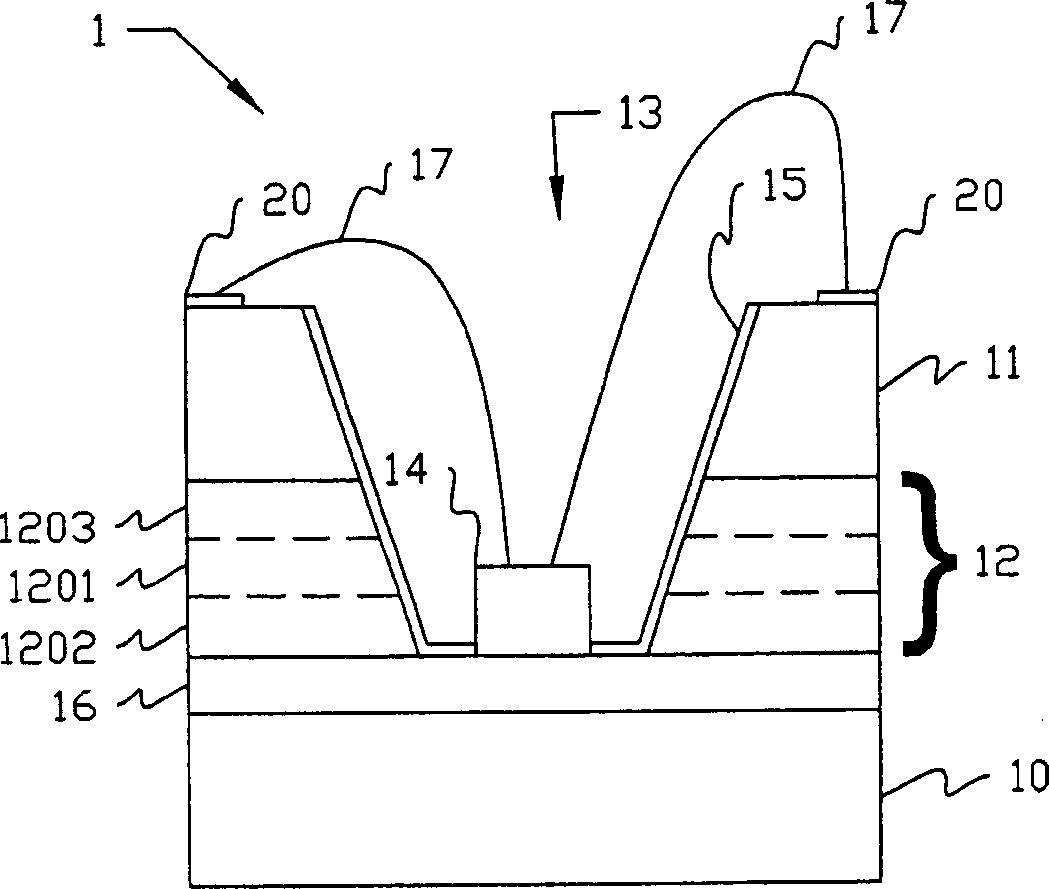
[0044] Figure 3a-3d A structural diagram showing a semiconductor light emitting element composition 1 according to another embodiment of the present invention. The mark 18 represents the light-transmitting material; 18a represents the filling material; 19 represents the wavelength conversion material.

[0045] The positive and negative electrodes of the semiconductor light emitting element 14 disclosed in the above embodiments are located on the same side, and the positive and negative electrodes are connected to the electrical contact 20 by wires 17 . However, the semiconductor light emitting device 14 in the present invention can also be a flip chip (Flip Chip) structure, that is, the positive and negative electrodes on the same side of the semiconductor light emitting device 14 are all facing the direction of the composite material substrate 10 . If the semiconductor light-emitting element 14 is configured in a flip-chip manner, the wire 17 is not needed, but the electric...


PUM


Abstract

The invention discloses a semiconductor luminous component, comprising a composite substrate, a circuit layout carrier, an adhesive structure, a sunk space and a semiconductor luminous component, where the adhesive structure is used to bond the composite substrate with the circuit layout carrier, the sunk space is formed on the circuit layout carrier and extends to the composite substrate , and the semiconductor luminous component is arranged in the sunk space and connected to the circuit layout carrier.

Description

technical field [0001] The invention relates to a packaging of a semiconductor light-emitting element. And in particular, it relates to a light-emitting element package made of composite material substrate and soft viscous material. Background technique [0002] US Patent No. 6,501,103 discloses a LED package, which includes a LED (12), a circuit board (2), and a heat dissipation base (3). Wherein, the light-emitting diode has a chip fixed on a cooling plate (10), and a welding pad electrically connected to a printed circuit board (13). The light emitting diode (12) is fixed on the circuit board (2) and the heat dissipation base (3). [0003] In this technology, the printed circuit board (13) and the cooling plate (10) are usually connected by mechanical means or soldering means. Mechanical methods, such as screws and buckles, require a relatively large area for disposing these mechanical devices, which is very unfavorable for electronic components that are increasingly m...

Claims


Application Information

Patent Timeline
Patent Type & Authority Applications(China)
IPC IPC(8): H01L33/00H05K1/02H01L33/64
CPCH01L2224/16225H01L2224/48091H01L2224/73265
Inventor 谢明勋殷寿志王健源王仁水蔡嘉芬许嘉良
Owner EPISTAR CORP
Why Eureka
Try Eureka