Tester and method for residual stress of seniconductor material

A technology of residual stress and testing equipment, which is applied in the field of semiconductors, can solve the problems of destroying the integrity of the material lattice, large measurement errors, and complicated and lengthy testing processes.

Inactive Publication Date: 2006-09-20
INST OF SEMICONDUCTORS - CHINESE ACAD OF SCI
View PDF0 Cites 22 Cited by
  • Summary
  • Abstract
  • Description
  • Claims
  • Application Information

AI Technical Summary

Problems solved by technology

Among them, the resistance strain gauge method and the mechanical extension method have relatively high measurement accuracy, but these two test methods are destructive and will destroy the lattice integrity of the material, and the measured stress is only the average value in a large range; X-ray diffraction Although the method does not damage the test material, its measurement error is relatively large, and because of its limited penetration depth, it can only test the residual stress of the surface layer or shallow layer; although the infrared polarimeter method requires a complicated and lengthy test process

Method used


Image

  • Tester and method for residual stress of seniconductor material
  • Tester and method for residual stress of seniconductor material
  • Tester and method for residual stress of seniconductor material

Examples


Embodiment

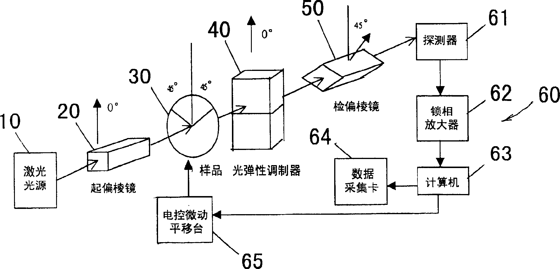
[0059] 1. Use laser diode pumped YAG solid-state laser light source with a wavelength of 1064nm.

[0060] 2. Put the 6-inch gallium arsenide wafer on the (001) plane into the testing system.

[0061] 3. Adjust the optical path and select the test point so that the polarization plane of the incident laser light is parallel to the surface of the test sample, and forms an included angle of 45 degrees with the directions [110] and [110] on the surface of the gallium arsenide wafer.

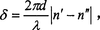
[0062] 4. Measure the strength-transmittance ratio difference ΔT / T in the [110] and [110] directions on the surface of the gallium arsenide wafer, and use the formula (1) described later to obtain the stress of the test point.

[0063] 5. Use computer programming to control the sample to automatically move to the next test point, repeat step 4, and measure the stress of this point.

[0064] 6. Step 5 is repeated until the entire GaAs wafer is tested to obtain the stress distribution of the entire GaA...


PUM


Abstract

This invention relates to a semiconductor material inner residual stress testing device. It includes a signal collecting system, the system is used to process the signal to get stress distributing situation of the sample. Optical bias checking prism, it is connected to collection system. Optical bias generating prism, it is set front of the checking prism. Optical elastic modulator, it is set between the two prisms. Laser source, it provides the signal source of the optical system.

Description

technical field [0001] The invention belongs to the technical field of semiconductors, in particular to a testing device and method for residual stress of semiconductor materials. Background technique [0002] Stress testing of semiconductor materials has always been one of the important means of material quality characterization. The size of the residual stress in the material directly reflects the quality of the material and the pros and cons of the preparation process. Materials with high residual stress will affect the quality of the epitaxially grown materials and degrade the performance of the devices prepared thereon. Therefore, the test of material stress has been widely concerned and valued, and it can provide reliable reference data for the growth process of modern materials in order to obtain better material quality. [0003] The commonly used stress testing methods before the present invention include the resistance strain gauge method, the mechanical extension...

Claims


Application Information

Patent Timeline
Patent Type & Authority Applications(China)
IPC IPC(8): G01N21/21G01N13/00
Inventor 陈涌海赵玲慧曾一平李成基
Owner INST OF SEMICONDUCTORS - CHINESE ACAD OF SCI
Why Eureka
Try Eureka