Printed circuit board capable of realizing high-speed signal transmission and making method

A printed circuit board, high-speed signal technology, applied in the direction of printed circuit manufacturing, printed circuit, circuit substrate materials, etc., can solve the problems of few applications, low signal test coverage, etc., achieve high-speed signal transmission, solve limitations, cost reduction effect

Inactive Publication Date:
View PDF0 Cites 35 Cited by
  • Summary
  • Abstract
  • Description
  • Claims
  • Application Information

AI Technical Summary

Problems solved by technology

[0042] In addition, the signal test coverage of the assembled finished board using the HDI process is relatively low. For example, through-hole test points cannot be used for test points in the area of ​​fine-pitch area array devices.
[0043] Based on the above defects, according to industry statistics, HDI printed boards are currently mainly used in mobile phone boards and packaging substrates, and are rarely used in large-scale system-level, high-reliability and complex printed boards.

Method used


Image

  • Printed circuit board capable of realizing high-speed signal transmission and making method
  • Printed circuit board capable of realizing high-speed signal transmission and making method
  • Printed circuit board capable of realizing high-speed signal transmission and making method

Examples


Embodiment Construction

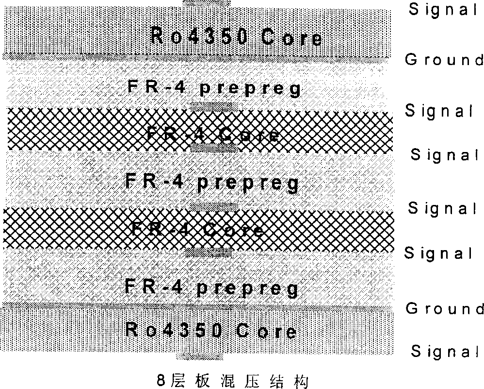
[0060] refer to figure 1 , figure 2 , image 3 , Figure 4 , Figure 5 , Figure 6 Generally, the high-speed signal transmission line on the PCB is only partial, and some layers of the PCB may not use high-grade materials, but the use price is relatively low, and the performance of the transmission signal is more common than ordinary materials such as FR4 to form multiple inner layers of the circuit board. , comprehensive signal quality requirements, simulation results and costs, and the maturity of the manufacturer's process, the plate mixed pressure technology can be used. Compared with the usual structure, the mixed pressure structure has more flexibility in terms of cost, performance, and availability. and adaptability, such as image 3 As shown, in order to realize the high-speed signal special board ROGERS4350 and the eight-layer board mixed structure of common board FR4: the two outer layers are made of ROGERS4350 special board that can transmit high-speed signals...


PUM


Abstract

The disclosed printing circuit board (PCB) is composed of two outer layers and one inner layer. The outer layer is made from plate of capable of transmitting signal in high speed; and the inner layer is made from general plate. Method for fabricating PCB includes following steps: carrying blackening / browning treatment; superimposing and pressing prepreg and outer copper foil together so as to form multilayer half finished board; drilling holes on multilayer board, plating via holes, using negative plate imaging and etching to prepare needed ducting lines in each core plate in inner layer; obtaining lines on outer layer so as to produce multilayer PCB in hybrid plates; back drilling technical holes in order to take out STUB with no connection and no attribute on end part of via holes. Features of the PCB are: high-speed signal transmission in low cost, high reliability, guaranteeing rate of good quality of PCB produced, and transmission quality of high-speed signal.

Description

technical field [0001] The invention relates to circuit board manufacturing technology, in particular to a printed circuit board for high-speed signal transmission, and also relates to a method for manufacturing the circuit board. Background technique [0002] At present, the design of high-speed PCB (printed circuit board) is widely used in communication, computer, graphics and image processing and other fields. All high-tech value-added electronic products are designed to pursue the characteristics of low power consumption, low electromagnetic radiation, high reliability, miniaturization, and light weight. In order to achieve the above goals, in high-speed PCB design, board materials and high-speed signal design become The key factor. [0003] Generally speaking, in order to meet the requirements of high-speed signals in design, in terms of design concept, the interconnection length between devices should be reduced as much as possible; in terms of network topology, it is...

Claims


Application Information

Patent Timeline
Patent Type & Authority Applications(China)
IPC IPC(8): H05K1/00H05K1/03H05K3/00H05K3/42H05K3/46
Inventor 黄春光
Why Eureka
Try Eureka