Lateral thin-film soi device having a field plate with isolated metallic regions

A metal area, lateral technology, applied in electrical components, semiconductor devices, circuits, etc., can solve problems such as uncertainty of lateral electric field, complexity, etc.

Inactive Publication Date: 2006-11-08
NXP BV
View PDF3 Cites 5 Cited by
  • Summary
  • Abstract
  • Description
  • Claims
  • Application Information

AI Technical Summary

Problems solved by technology

From this, the transverse electric field is determined by the design of the capacitive field electrode chain, which is therefore complex in the element design
Doping in the drift region does not determine the lateral electric field

Method used


Image

  • Lateral thin-film soi device having a field plate with isolated metallic regions
  • Lateral thin-film soi device having a field plate with isolated metallic regions

Examples


Embodiment Construction

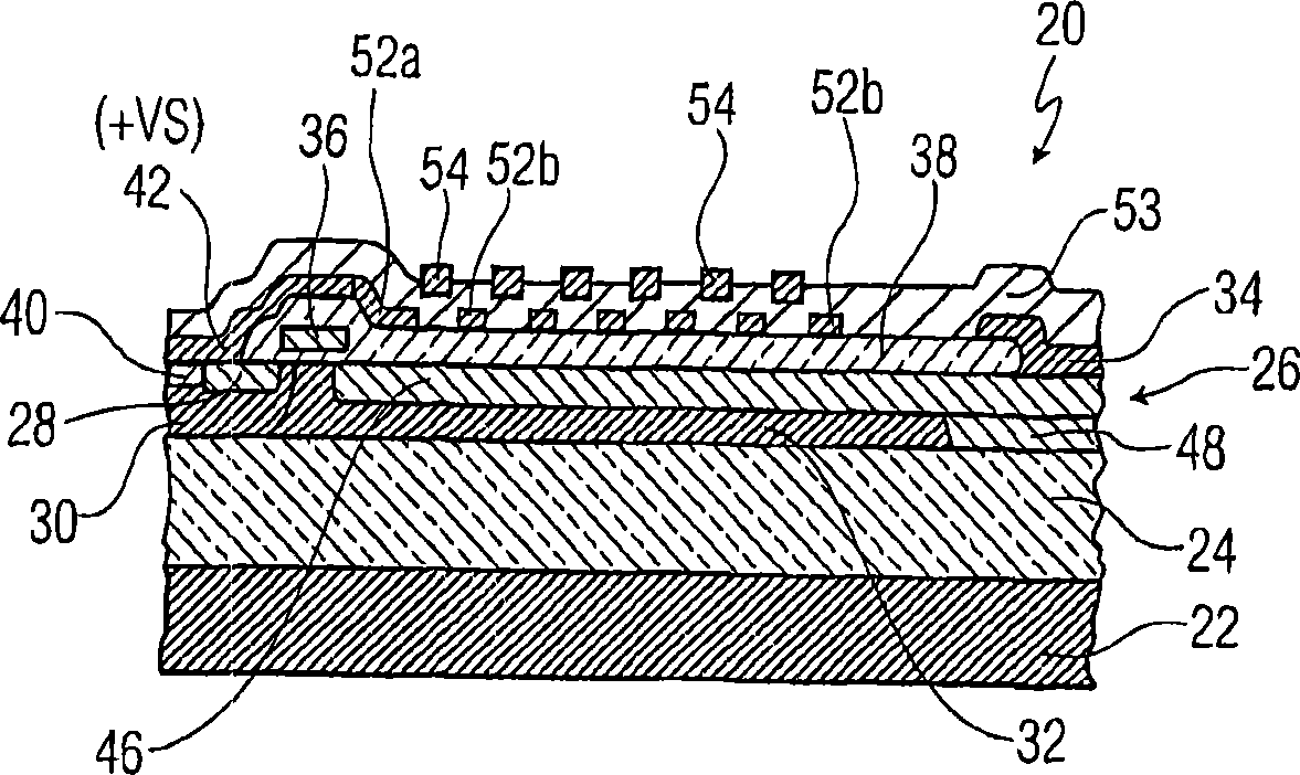
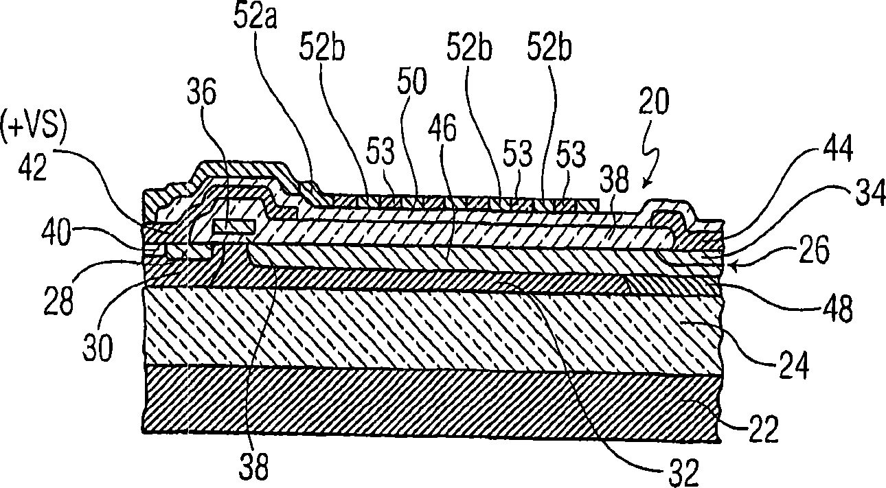
[0014] like figure 1 As shown, a lateral thin film device, here an SOI PMOS transistor 20, includes a semiconductor substrate 22, a buried insulating layer 24, and a semiconductor surface SOI layer 26 in which the device is fabricated. The PMOS transistor includes a source region 28 of p-type conductivity, a body region 30 of n-type conductivity, a lateral drift region 32 of n-type conductivity and a drain region 34 of p-type conductivity. The device also includes a gate electrode 36 which is fully insulated from the underlying semiconductor surface layer 26 and other conductive parts of the device by an oxide isolation region 38 . In addition, transistor 20 includes a body contact surface region 40 , a surface bonded drain extension 46 of p-type conductivity, a source contact electrode 42 connected to a high voltage +Vs, and a drain contact electrode 44 .

[0015] The field electrodes are provided such that they extend laterally and substantially cover the lateral drift regi...


PUM


Abstract

In a lateral thin-film Silicon-On-Insulator (SOI) device, a field plate is provided to extend substantially over a lateral drift region to protect the device from package and surface charge effects. In particular, the field plate comprises a layer of plural metallic regions which are isolated laterally from one another by spacing so as to assume a lateral electric field profile which is established by a volume doping gradient in the silicon drift region.

Description

technical field [0001] The present invention relates to semiconductor-on-insulator (SOI) devices and, more particularly, to field electrodes for use in such devices having laterally isolated metal regions that form a linear lateral electric field to eliminate field enhancement. Background technique [0002] Field electrodes are used in semiconductor-on-insulator (SOI) devices to protect the drift region of the device from packaging and surface charges that may be caused by moisture or other containment on the wafer surface. Field electrodes are typically constructed of metallic material and are connected to, or are extensions of, the source or gate electrodes, as described in US Patent Nos. 6,127,703 and 5,412,241, which are hereby incorporated by reference into this application . [0003] However, such a field electrode causes an electric field enhancement at the edge of the field electrode, leading to injection of electrons into the interlayer dielectric. This problem is...

Claims


Application Information

Patent Timeline
Patent Type & Authority Applications(China)
IPC IPC(8): H01L29/06H01L29/40H01L29/417H01L29/786
CPCH01L29/404H01L29/405H01L29/41733H01L29/7835H01L29/78624H01L29/41725
Inventor T·莱塔维克
Owner NXP BV
Why Eureka
Try Eureka