Preparation method for power device structure, and structure

A technology for power devices and polysilicon, which is used in the manufacture of semiconductor/solid-state devices, semiconductor devices, electrical components, etc. It can solve the problems of limited improvement in device performance, increased device reliability, and high surface electric field of devices

Active Publication Date: 2015-11-18
工业和信息化部电子第五研究所华东分所
View PDF5 Cites 0 Cited by
  • Summary
  • Abstract
  • Description
  • Claims
  • Application Information

AI Technical Summary

Problems solved by technology

Traditional lateral RESURFSOI technologies, such as field plate technology, thin silicon film technology, etc., have improved the electric field in the middle of the drift region to a certain extent, but the improvement in device performance is limited, and the surface electric field of the device is higher, which increases the reliability of the device during use. sexual problems

Method used


Image

  • Preparation method for power device structure, and structure
  • Preparation method for power device structure, and structure
  • Preparation method for power device structure, and structure

Examples


Embodiment 1

[0034] refer to figure 1 , figure 1 It is a schematic flow chart of the preparation method of the power device structure according to the embodiment of the present invention.

[0035] In Embodiment 1, the preparation method of the power device structure includes:

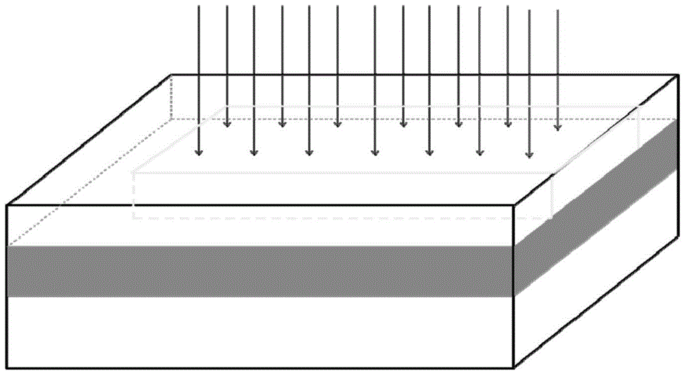
[0036] Step 101, perform phosphorus implantation on the thin-film SOI wafer, perform high-temperature annealing, activate implanted ions, perform silicon etching, until the buried oxide layer is formed to form SiO 2 Dielectric window, made of SiO 2 deposited, SiO 2 Etching, until the surface of the buried oxide layer, forming a polysilicon window for polysilicon deposition;

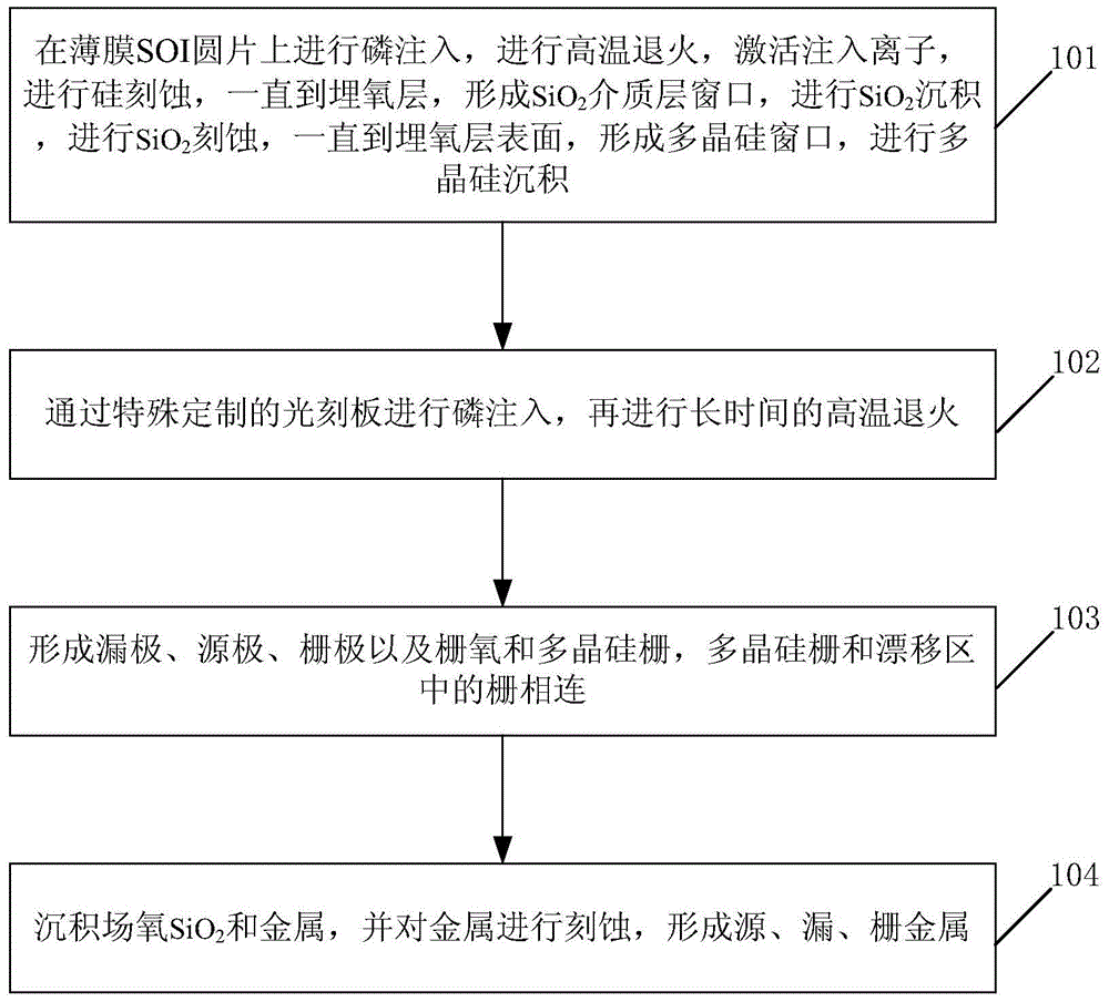
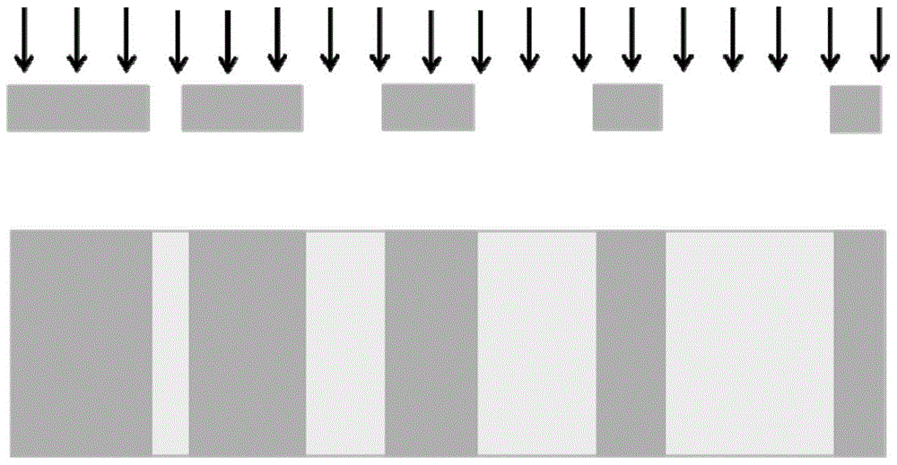
[0037] Step 102, performing phosphorus implantation through a specially customized photolithography plate, and then performing long-term high-temperature annealing;

[0038] Specifically, the lithograph reference figure 2 as shown, figure 2 It is a schematic structural diagram of a photoresist plate provided by an embodiment of the pre...

Embodiment 2

[0053] refer to Figure 10 , Figure 10 is a schematic diagram of the power device structure of the embodiment of the present invention.

[0054] In Embodiment 2, the power device structure includes:

[0055] P-type substrate, buried oxide layer, source, gate, n-type offset region, linear doped polysilicon layer, heavily doped n-type layer, SiO 2 and drain;

[0056] The P-type substrate is at the bottom of the power device, the buried oxide layer is on the P-type substrate, and the doping concentration inside the linearly doped polysilicon changes from that near the source to gradually increases from one end to the end near the drain, linearly distributed, and the SiO 2 An n-type layer with high doping concentration is formed on both sides of the groove.


PUM


Abstract

The embodiment of the invention discloses a preparation method for a power device structure, and the method comprises the steps: injecting phosphorus onto a thin film SOI wafer, carrying out high-temperature annealing, activating injected ions, and carrying out heavy doping of an n-type drift region from the surface of the device to the upper surface of a buried oxide layer; carrying out silicon etching till the buried oxide layer, forming a SiO2 dielectric layer window, carrying out SiO2 deposition, carrying out SiO2 etching till the surface of the buried oxide layer, forming a polycrystalline silicon window, and carrying out polycrystalline silicon deposition; carrying out phosphorus injection through a specially-customized photoetching plate, and then carrying out long-time high-temperature annealing; forming a drain electrode, a source electrode, a grid electrode, a gate-oxide, and a polysilicon gate, wherein the polysilicon gate is connected with a gate in the drift region; depositing field oxide SiO2 and metal, carrying out the etching of the metal, and forming source, drain and grid metal, thereby effectively improving the breakdown voltage of a device, and reducing the conduction resistance of the device.

Description

technical field [0001] Embodiments of the present invention relate to the technical field of semiconductor devices, and in particular to a method and structure for preparing a power device structure. Background technique [0002] Power integrated circuits are sometimes called high-voltage integrated circuits, which are an important branch of modern electronics. They can provide new circuits with high speed, high integration, low power consumption and radiation resistance for various power conversion and energy processing devices, and are widely used in electric power Daily consumption fields such as control systems, automotive electronics, display device drivers, communications and lighting, as well as many important fields such as national defense and aerospace. The rapid expansion of its application scope has also put forward higher requirements for the high-voltage devices in its core part. [0003] For the power device MOSFET, first, under the premise of ensuring the br...

Claims


Application Information

Patent Timeline
Patent Type & Authority Applications(China)
IPC IPC(8): H01L21/336H01L29/78H01L29/06
CPCH01L29/06H01L29/0607H01L29/0611H01L29/66681H01L29/7816
Inventor 夏超张琦
Owner 工业和信息化部电子第五研究所华东分所
Why Eureka
Try Eureka