A method for removing silicon defects in the top layer of tm-soi

A TM-SOI, top-layer silicon technology, used in electrical components, circuits, semiconductor/solid-state device manufacturing, etc., can solve problems such as atomic displacement, affecting SOI quality, and achieve the effect of reducing particles, improving roughness, and improving cleanliness

Active Publication Date: 2021-05-07
SHENYANG SILICON TECH
View PDF4 Cites 0 Cited by
  • Summary
  • Abstract
  • Description
  • Claims
  • Application Information

AI Technical Summary

Problems solved by technology

[0005] From the perspective of surface flatness, the CMP process effectively improves the roughness of the SOI stripped surface and removes the damaged layer on the surface. However, during ion implantation, the ions inevitably collide with the lattice atoms in the material, resulting in atomic displacement, resulting in a large number of defects
When the dose of ion implantation is high, these defects can also overlap and interact to produce more complex defects
These defects have an important impact on the electrical characteristics and seriously affect the quality of SOI
These problems cannot be solved by relying solely on the CMP process.
[0006] Therefore, using TM-SOI technology and CMP technology to completely remove the damaged layer after the split, repair the defects in the top silicon layer of TM-SOI, and reduce the roughness, there are great process problems and technical difficulties.

Method used


Image

  • A method for removing silicon defects in the top layer of tm-soi
  • A method for removing silicon defects in the top layer of tm-soi
  • A method for removing silicon defects in the top layer of tm-soi

Examples


Embodiment 1

[0049] Using TM-SOI technology, 3 pieces of SOI wafer materials with a diameter of 200mm after splitting were prepared, and they were placed in the reaction chamber of the epitaxy furnace for corrosion and defect repair. The specific steps are as follows:

[0050] (1) H is introduced into the reaction chamber 2 (Flow rate 50 liters / minute, purity>99.99999%), heating at 1050°C for 30 seconds, removing the natural oxide layer and impurities on the surface of the silicon wafer in situ;

[0051] (2) reduce the pressure of the reaction chamber, and the pumping pressure reaches 40torr, and the SOI silicon wafer processed through step (1) is placed in an anhydrous HCl atmosphere to corrode the silicon layer on its surface for 60 seconds;

[0052] (3) The reaction chamber is refilled with H 2 (flow rate 20 liters / minute, purity>99.99999%), restore the pressure of the reaction chamber to normal pressure, remove impurities and residual HCl in the reaction chamber, cool to the loading t...

Embodiment 2

[0063] Two pieces of the same batch of SOI wafer material as in Example 1 were taken and placed in the reaction chamber of an epitaxial furnace for HCl corrosion and defect repair. The different conditions from Example 1 are that the corrosion temperature is 850° C., the pumping pressure reaches 20 torr, and the corrosion is performed for 120 seconds. Table 3 is the test data:

[0064] table 3

[0065]

[0066]

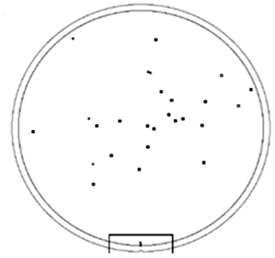
[0067] After being processed under this condition, the measured particle results are shown in Table 4, and the particle diagram is shown in image 3 , Figure 4 shown.

[0068] Table 4

[0069]

Embodiment 3

[0079] 10 SOI sheets in Example 1, Example 2, Comparative Example 1 and Comparative Example 2 were subjected to SECCO corrosion (pure water, 49% HF, potassium dichromate) for 20s, and then observed under an optical microscope to obtain The results are shown in Table 7:

[0080] Table 7

[0081] Numbering Number of defects (ea / cm 2 )

[0082] From the comparison of the data in Table 7, it can be seen that the method adopted in the present invention is obviously superior to the CMP process in terms of defect removal.


PUM


Abstract

The invention discloses a method for removing silicon defects in the top layer of TM-SOI, belonging to the technical field of SOI preparation. The method is to chemically etch the SOI silicon wafer formed by TM-SOI to remove the damaged layer on the surface of the thin-film SOI silicon wafer. After repairing, high-quality SOI silicon wafers are obtained. The SOI prepared by this method can not only improve the surface roughness, but most importantly, can repair SOI defects, and prepare SOI materials with excellent electrical properties.

Description

technical field [0001] The invention relates to the technical field of SOI, in particular to a method for removing silicon defects in the top layer of TM-SOI (Silicon on Insulator, silicon on insulator). Background technique [0002] TM-SOI is a kind of SOI technology based on the ion implantation stripping method (smart-cut method). The "TM-SOI smart-cut method" has applied for an invention patent in China with the application number 200310123080.1, and has obtained the invention patent authorization from the China Patent Office. The specific method: form an oxide film on at least one of the two silicon wafers, and use ion implantation to form an ion separation layer in the thin film of one of the silicon wafers, so that the ion-implanted surface is separated from the oxide film. The film is bonded to the other silicon wafer at room temperature to form a bonded body. Then it is annealed to make the bonding surface firm. Then raise the temperature to above the transition t...

Claims


Application Information

Patent Timeline
Patent Type & Authority Patents(China)
IPC IPC(8): H01L21/762H01L21/322
CPCH01L21/3226H01L21/76254
Inventor 高文琳柳清超孙伟
Owner SHENYANG SILICON TECH
Why Eureka
Try Eureka