Ceramic substrate and its manufacturing method

A technology of ceramic substrates and manufacturing methods, which is applied in the fields of printed circuit manufacturing, circuit substrate materials, semiconductor/solid-state device manufacturing, etc., can solve the problems of complicated production process and unfavorable mass production, etc., and achieve reduction of plane shrinkage rate and reduction of shrinkage rate , Increase the effect of heat transfer rate

Inactive Publication Date: 2006-11-29
DELTA ELECTRONICS INC
View PDF1 Cites 4 Cited by
  • Summary
  • Abstract
  • Description
  • Claims
  • Application Information

AI Technical Summary

Problems solved by technology

Or add a layer of alumina on the top and bottom of the ceramic layer, provide friction during the sintering process to limit the shrinkage of the ceramic layer, and then remove the alumina after the sintering process is over, but the above methods will complicate the overall production process and It is not conducive to mass production, so when factors such as sintering temperature, shrinkage characteristics and electrical characteristics are considered at the same time, and it is hoped to simplify the process to reduce manufacturing costs, a ceramic substrate and its manufacturing method that meet industry needs and reduce shrinkage are provided. It is indeed one of the important issues at present

Method used


Image

  • Ceramic substrate and its manufacturing method
  • Ceramic substrate and its manufacturing method
  • Ceramic substrate and its manufacturing method

Examples


Embodiment Construction

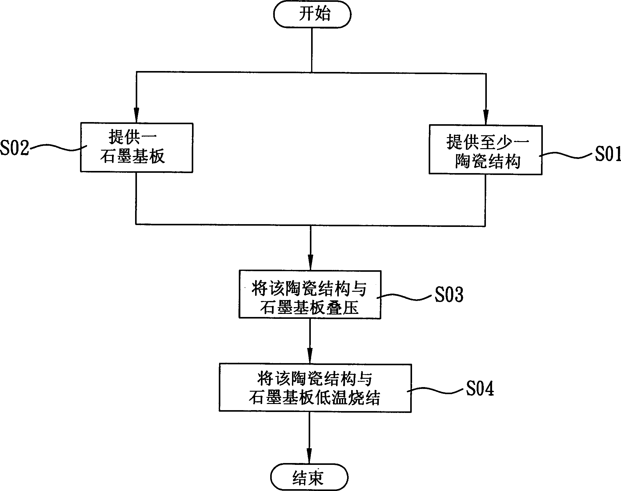
[0027] A ceramic substrate according to a preferred embodiment of the present invention will be described below with reference to related drawings.

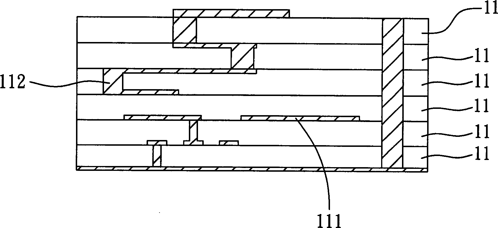
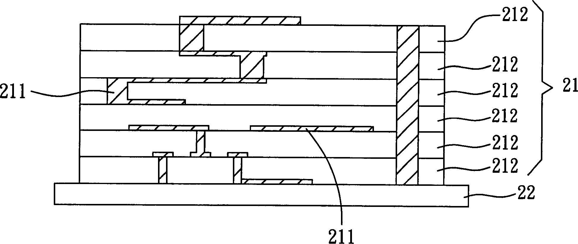
[0028] Please refer to figure 2 Shown is a cross-sectional view of a ceramic substrate in a preferred embodiment of the present invention. The ceramic substrate 2 of the preferred embodiment of the present invention includes at least one ceramic structure 21 and a graphite substrate 22 .

[0029] The ceramic structure 21 can be prepared by mixing different proportions of ceramic powder and glass powder, and appropriate raw materials can be selected according to the required thermal expansion coefficient or other process parameters. Generally speaking, the raw materials of the ceramic structure 21 include alumina, quartz, calcium zirconate (CaZrO 3 ), forsterite (Mg 3 SiO 4 ), silica, andalusite, silicon dioxide, calcium borosilicate glass (Borosilicate Glass), etc., or other raw materials that can be used as ceramics.

[00...


PUM

PropertyMeasurementUnit
densityaaaaaaaaaa

Abstract

A making method of ceramic substrate includes the following steps: providing at least one graphite substrate and a ceramic structure, then overlapping the ceramic and graphite substrate and sintering the layers of ceramic substrate and graphite structure finally. In addition, the invention also provides a ceramic substrate consisting of at least one ceramic substrate and one graphite structure, and the ceramic substrate is formed by sintering the aforementioned structural layers.

Description

technical field [0001] The invention relates to a ceramic substrate and a manufacturing method thereof, in particular to a ceramic substrate with a graphite substrate and a manufacturing method thereof. Background technique [0002] With the advancement of science and technology, the current electronic products are developing towards miniaturization and thinning. For example, personal mobile communication products in the wireless communication industry are for example. In just a few years, the size of personal mobile communication products has shrunk from the earliest handheld to the current palm. Large or even small enough to be put into a watch, its function has evolved from the simplest voice transmission to the ability to transmit data, text, light, thin, short, small, and multi-functions are the focus of current design of personal mobile communication products. trend. Low Temperature Co-fired Ceramics (LTCC) is a technology that can meet this demand. Low-temperature c...

Claims


Application Information

Patent Timeline
Patent Type & Authority Applications(China)
IPC IPC(8): H05K1/03H05K3/00
CPCH05K3/4629H01L2924/0002H05K1/053H01L23/15H05K1/0306H01L21/4857H05K3/4611H01L2924/09701H05K2201/0323Y10T428/30H01L2924/00
Inventor 彭俊维眭明山
Owner DELTA ELECTRONICS INC
Why Eureka
Try Eureka