
Plasma processing chamber, potential controlling apparatus, method, program and storage medium

A plasma and potential control technology, which is applied in plasma, ion implantation plating, semiconductor/solid-state device manufacturing, etc., can solve the problems of reduced working efficiency, difficult control, and difficult control of side wall potential in plasma processing chambers, etc. Achieve the effect of preventing the reduction of work efficiency, simplifying the structure, and preventing consumption

Active Publication Date: 2006-12-06
TOKYO ELECTRON LTD
View PDF1 Cites 8 Cited by
  • Summary
  • Abstract
  • Description
  • Claims
  • Application Information

AI Technical Summary

Problems solved by technology

[0005] However, since the potential of the side wall is determined by the anode / cathode ratio influenced by the electrode and the shape of the side wall and the magnitude of the high-frequency power set in order to obtain the desired plasma processing result on the semiconductor wafer, the potential of the side wall is controlled it is hard
Therefore, it is not easy to control the removal of the polymer. If the polymer is attached to the side wall and the deposition process of easy-attachment deposition is repeated on the surface of the semiconductor wafer, the amount of polymer attachment is too large, so it is necessary to improve the cleaning of the side wall. frequency, and as a result, the efficiency of the plasma processing chamber is reduced

Method used


Image

  • Plasma processing chamber, potential controlling apparatus, method, program and storage medium
  • Plasma processing chamber, potential controlling apparatus, method, program and storage medium
  • Plasma processing chamber, potential controlling apparatus, method, program and storage medium

Examples


Embodiment Construction

[0074] Hereinafter, embodiments of the present invention will be described with reference to the drawings.

[0075] First, a plasma processing chamber according to a first embodiment of the present invention will be described.

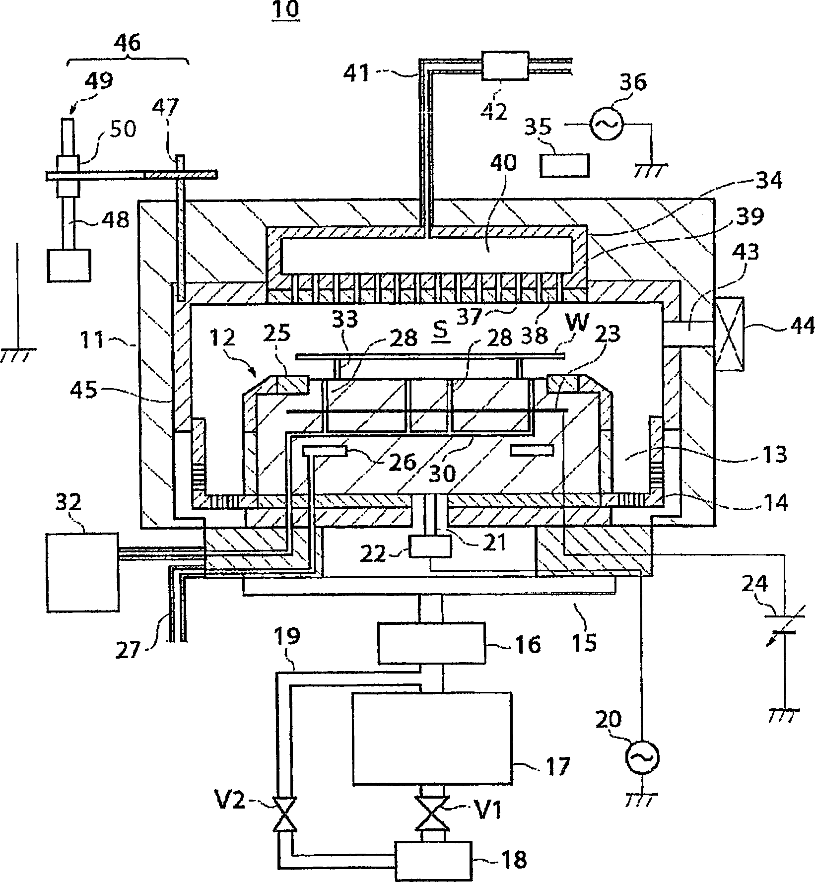
[0076] figure 1 is a cross-sectional view showing a schematic configuration of a plasma processing chamber according to this embodiment. This plasma processing chamber is configured to perform RIE (Reactive Ion Etching) processing and ashing processing on a semiconductor wafer W serving as a substrate.

[0077] figure 1 Among them, the plasma processing chamber 10 has a cylindrical container 11, and in the container 11, a columnar wafer W (hereinafter simply referred to as "wafer W") as a mounting table with a diameter of 300 mm is disposed. base 12.

[0078] In the plasma processing chamber 10 , an exhaust path 13 serving as a flow path for exhausting gas molecules above the susceptor 12 to the outside of the vessel 11 is formed through the inner ...


PUM


Abstract

The invention relates to a plasma processing chamber (10) which comprises a covered container (11), cylinder side wall component (45) inside the container, an electric potential control device (46) with conducting component (47) which can be contacted with the side wall component (45), or not be contacted with the side wall component (45) and be grounded via up and down. During the RIE process, the conducting component (47) is contacted with the side wall component (45) via lowering down, setting the electric potential of the side wall component (45) as grounding potential; during the ashing process, the conducting component (47) is not contacted with the side wall component (45) via rising up, setting the electric potential of the side wall component (45) as suspension joint electric potential.

Description

technical field [0001] The present invention relates to a plasma processing chamber, a potential control device, a potential control method, a program, and a storage medium, and particularly to a plasma processing chamber having components exposed to plasma. Background technique [0002] Conventionally, a plasma processing chamber including a cylindrical container and an electrode arranged in the container and connected to a high-frequency power source is known. In this plasma processing chamber, a processing gas is introduced into a container, and high-frequency power is applied to electrodes in a space in the container. Furthermore, when a semiconductor wafer serving as a substrate is housed in a container, the introduced processing gas is turned into plasma by high-frequency power to generate ions, and the semiconductor wafer is subjected to plasma processing, such as etching processing, by the ions. [0003] In the above-mentioned plasma processing chamber, when the rea...

Claims


Application Information

Patent Timeline
Patent Type & Authority Applications(China)
IPC IPC(8): H01L21/00H01L21/205H01L21/3065H01L21/31H01L21/67C23C16/00C23C14/00C23F4/00H01J37/32H05H1/00
Inventor 本田昌伸速水利泰
Owner TOKYO ELECTRON LTD
Learn More