Plasma processing chamber, potential controlling apparatus, method, program and storage medium

A plasma and potential control technology, applied in the fields of plasma, ion implantation and plating, semiconductor/solid-state device manufacturing, etc. The effect of preventing the reduction of work efficiency, preventing consumption, and simple structure

Active Publication Date: 2008-07-09
TOKYO ELECTRON LTD
View PDF4 Cites 0 Cited by
  • Summary
  • Abstract
  • Description
  • Claims
  • Application Information

AI Technical Summary

Problems solved by technology

[0008] However, in the processing chamber of Patent Document 1, in addition to the high-frequency power supply for the electrodes, a high-frequency power supply for the side walls is also required, that is, a high-frequency power supply for the components of the processing chamber other than the electrodes, so the processing chamber The composition of the problem becomes complicated
[0009] In addition, in the processing chamber of Patent Document 1, when the operating time reaches a predetermined value, only the polymer on the side wall is removed by connecting the side wall to the high-frequency power supply, so it is difficult to control the amount of polymer adhesion. As a result, in a plasma In the processing chamber, when repeating the above deposition process and using O 2 Gas is used as a processing gas, no neutral active radicals are generated, no polymer is attached to the side wall, and no deposition is attached to the surface of the semiconductor wafer. If the polymer on the side wall is to be completely removed, there will also be Possibility that positive ions collide directly with the side wall without polymer, and consume the side wall, and as a result, the working efficiency of the plasma processing chamber decreases.

Method used


Image

  • Plasma processing chamber, potential controlling apparatus, method, program and storage medium
  • Plasma processing chamber, potential controlling apparatus, method, program and storage medium
  • Plasma processing chamber, potential controlling apparatus, method, program and storage medium

Examples


Embodiment Construction

[0071] Hereinafter, embodiments of the present invention will be described with reference to the drawings.

[0072] First, a plasma processing chamber according to a first embodiment of the present invention will be described.

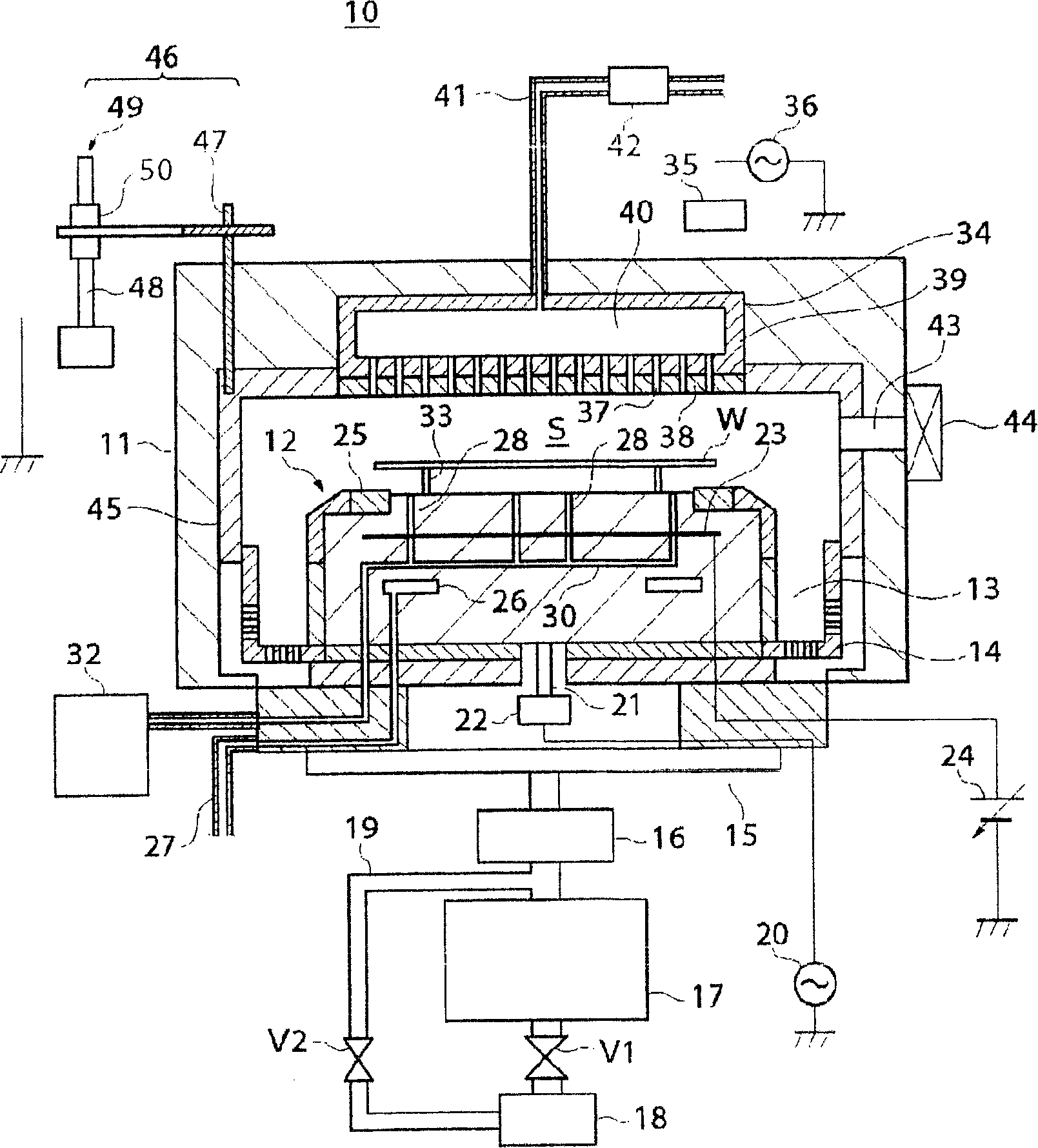
[0073] figure 1 is a cross-sectional view showing a schematic configuration of a plasma processing chamber according to this embodiment. This plasma processing chamber is configured to perform RIE (Reactive Ion Etching) processing and ashing processing on a semiconductor wafer W serving as a substrate.

[0074] figure 1 Among them, the plasma processing chamber 10 has a cylindrical container 11, and in the container 11, a columnar wafer W (hereinafter simply referred to as "wafer W") as a mounting table with a diameter of 300 mm is disposed. base 12.

[0075] In the plasma processing chamber 10 , an exhaust path 13 serving as a flow path for exhausting gas molecules above the susceptor 12 to the outside of the vessel 11 is formed through the inner ...


PUM


Abstract

The invention relates to a plasma processing chamber (10) which comprises a covered container (11), cylinder side wall component (45) inside the container, an electric potential control device (46) with conducting component (47) which can be contacted with the side wall component (45), or not be contacted with the side wall component (45) and be grounded via up and down. During the RIE process, the conducting component (47) is contacted with the side wall component (45) via lowering down, setting the electric potential of the side wall component (45) as grounding potential; during the ashing process, the conducting component (47) is not contacted with the side wall component (45) via rising up, setting the electric potential of the side wall component (45) as suspension joint electric potential.

Description

technical field [0001] The present invention relates to a plasma processing chamber, a potential control device, a potential control method, a program, and a storage medium, and particularly to a plasma processing chamber having components exposed to plasma. Background technique [0002] Conventionally, a plasma processing chamber including a cylindrical container and an electrode arranged in the container and connected to a high-frequency power source is known. In this plasma processing chamber, a processing gas is introduced into a container, and high-frequency power is applied to electrodes in a space in the container. Furthermore, when a semiconductor wafer serving as a substrate is housed in a container, the introduced processing gas is turned into plasma by high-frequency power to generate ions, and the semiconductor wafer is subjected to plasma processing, such as etching processing, by the ions. [0003] In the above-mentioned plasma processing chamber, when the rea...

Claims


Application Information

Patent Timeline
Patent Type & Authority Patents(China)
IPC IPC(8): H01L21/00H01L21/205H01L21/3065H01L21/31H01L21/67C23C16/00C23C14/00C23F4/00H01J37/32H05H1/00
Inventor 本田昌伸速水利泰
Owner TOKYO ELECTRON LTD
Why Eureka
Try Eureka