Envelope for luminous elements of semiconductor in large power

A technology of light-emitting components and semiconductors, applied in semiconductor devices, semiconductor/solid-state device parts, electrical components, etc., can solve the problem of small contact area between LED light-emitting chip and heat dissipation carrier, no complete improvement of heat dissipation efficiency, and large heat pipe volume. and other problems, to achieve the effect of improving refrigeration efficiency, small size and saving volume

Active Publication Date: 2011-08-17
DAJIN ORIENT LIGHTING SHENZHEN
View PDF2 Cites 0 Cited by
  • Summary
  • Abstract
  • Description
  • Claims
  • Application Information

AI Technical Summary

Problems solved by technology

Chinese patent specification CN 1664433A discloses a method of heat dissipation using heat pipes. Compared with ordinary heat sinks, the thermal resistance of heat dissipation has been reduced. However, due to the large volume of heat pipes, the design of heat sinks is limited by the shape of heat pipes. Due to LED The contact area between the light-emitting chip and the heat dissipation carrier is objectively quite small, and the heat of the LED is passively conducted through the convection of the heat pipe, so the heat dissipation efficiency has not been completely improved, and the structure of the heat pipe requires a large volume, which affects the actual application.

Method used


Image

  • Envelope for luminous elements of semiconductor in large power
  • Envelope for luminous elements of semiconductor in large power
  • Envelope for luminous elements of semiconductor in large power

Examples


Embodiment Construction

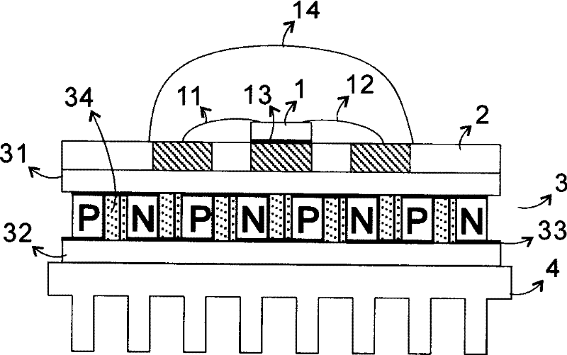
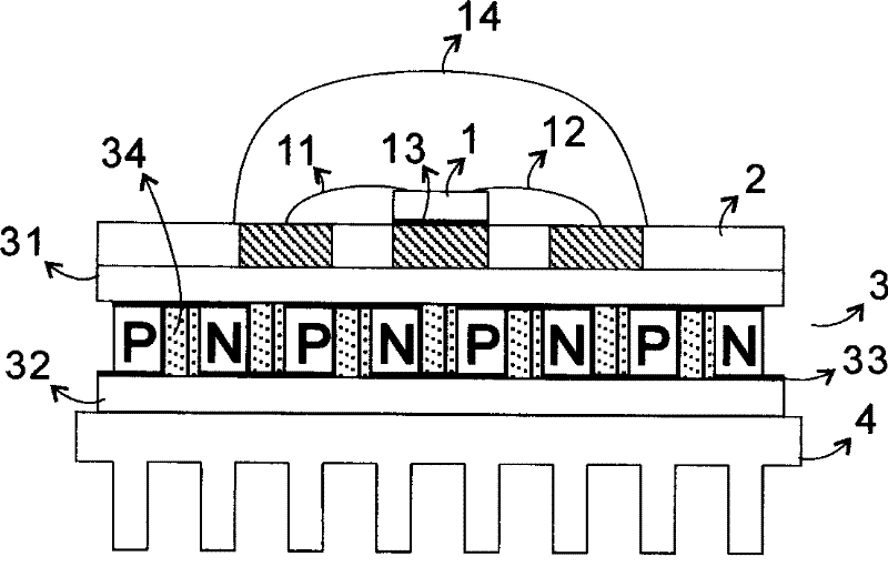
[0022] Hereinafter, preferred embodiments of the present invention will be described with reference to the accompanying drawings. With reference to the drawings, wherever possible, the same reference numbers will be used throughout the drawings to refer to the same or like parts. Also, it is considered that detailed descriptions of known functions and structures of key points of the present invention will be omitted.

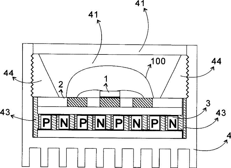
[0023] figure 1 It is a cross-sectional view of the high-power semiconductor light-emitting element package of the present invention. The high-power semiconductor light-emitting element package includes at least one LED chip 1 electrically connected inside and outside; an LED substrate 2, and each of the at least one or more LED chips 1 is fixed on the front side of the substrate 2. , LED chip 1 is packaged with silicon material or epoxy resin. Wherein, each LED chip 1 provided with internal and external electrical connections is bonded to an external circuit ...


PUM


Abstract

The disclosed package includes following parts and structures: at least one inner and outer connected LED chip electrically; LED base plate and at least more than one LED chips, and each LED chip is fixed on front face of base plate; underside of base plate is jointed to electronic refrigerating chip in semiconductor; the refrigerating chip possesses a cold end and a heat end; the cold end is jointed to the underside of base plate, and the heat end is formed thermal contact to thermolysis bottom seat. Comparing with packaging technique in passive thermolysis mode such as traditional thermal fins and heat pipe etc, the disclosed package absorbs a great lot quantity of heat generated from semiconductor luminescence chip in large power forwardly and quickly so as to provide thermolysis channel in high performance between LED luminescence chip and radiating carrier.

Description

technical field [0001] The present invention relates to the packaging of high-power semiconductor light-emitting element LED, in particular to a packaging structure for effectively dissipating the heat generated during the operation of the semiconductor light-emitting element LED. Background technique [0002] The application of high-power and high-brightness LEDs (light-emitting diodes) continues to expand, first entering the field of special lighting, and moving towards general lighting. Due to the continuous improvement of the output power of LED chips, higher requirements are put forward for the packaging structure of high-power LEDs. The traditional LED packaging structure is generally made by using conductive or non-conductive glue to mount the chip in a small-sized reflector cup or on a wafer stage, and then encapsulating the device with epoxy resin after completing the internal and external connections of the device with gold wires. If the high-power LED adopts the ...

Claims


Application Information

Patent Timeline
Patent Type & Authority Patents(China)
IPC IPC(8): H01L25/075H01L25/00H01L23/34H01L23/38
CPCH01L2224/45144H01L2224/48091H01L2224/73265
Inventor 朱建钦
Owner DAJIN ORIENT LIGHTING SHENZHEN
Why Eureka
Try Eureka