Test equipment of semiconductor devices

An inspection device and semiconductor technology, applied in the direction of single semiconductor device testing, semiconductor/solid-state device testing/measurement, measuring devices, etc., can solve the problems of rising prices and increasing the proportion of test costs, and achieve the increase of transition reaction speed and test The effect of shortening the time and reducing the influence of motion noise

Active Publication Date: 2006-12-13
ADVANTEST CORP
View PDF3 Cites 9 Cited by
  • Summary
  • Abstract
  • Description
  • Claims
  • Application Information

AI Technical Summary

Problems solved by technology

[0007] Here, with the increase in the speed of semiconductor devices, the price of semiconductor device inspection equipment such as burn-in equipment and memory testers has risen, and the proportion of test costs in the sales price of semiconductor devices has greatly increased.

Method used


Image

  • Test equipment of semiconductor devices
  • Test equipment of semiconductor devices
  • Test equipment of semiconductor devices

Examples


Embodiment Construction

[0049] Hereinafter, preferred forms for carrying out the present invention will be described more specifically with reference to the accompanying drawings. Here, in the drawings, the same components are assigned the same reference numerals, and redundant descriptions are omitted. Furthermore, since the description herein is of a preferred form of carrying out the invention, the invention is not limited to this form.

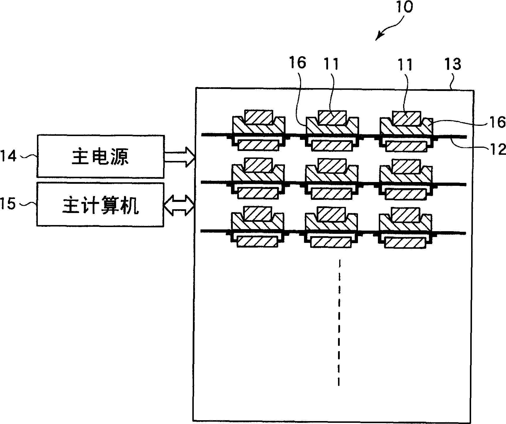
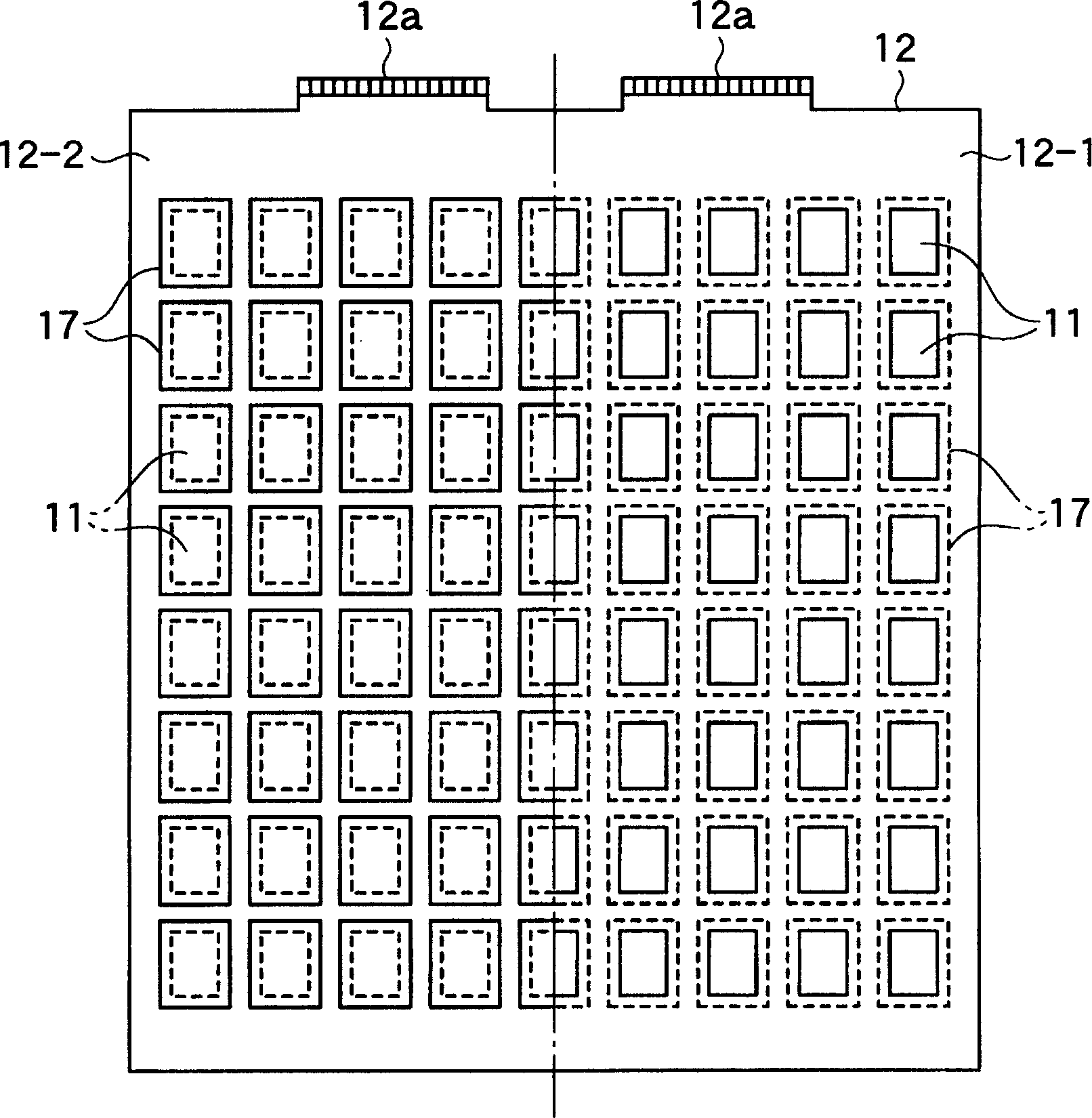
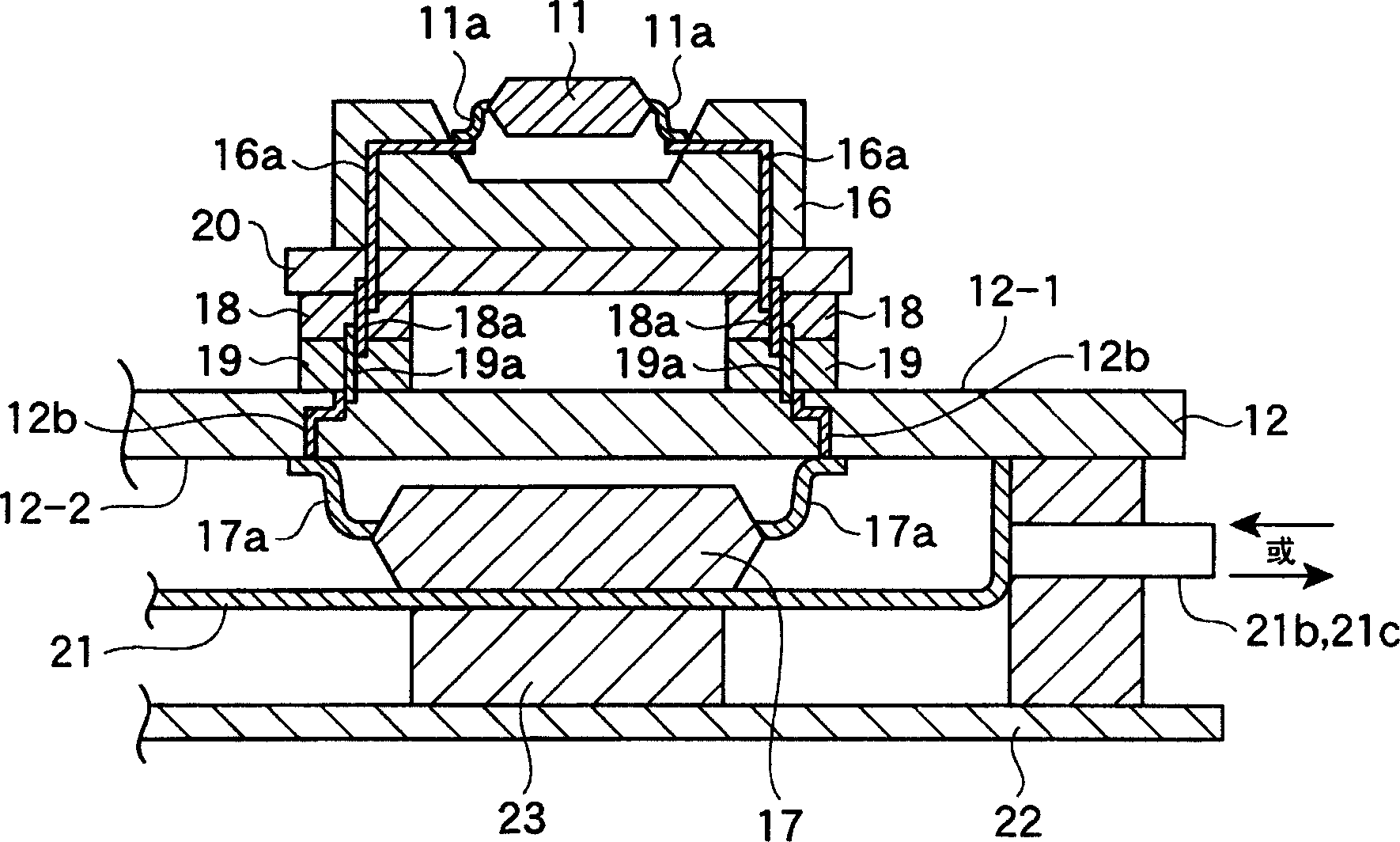
[0050] figure 1 is a conceptual diagram showing an inspection device for a semiconductor device according to an embodiment of the present invention, figure 2 for expressing in figure 1 An explanatory diagram of a test board accommodated in a cavity in an inspection device for a semiconductor device, image 3 for figure 2 A cross-sectional view of the test plate, Figure 4 Fig. 5 is a block diagram showing the functional structure of the device testing mechanism mounted on the test board, which is a perspective view showing the cooling mechanism mounted on ...


PUM


Abstract

The invention provides a detection device for reducing the test cost of semicondustor device. An test equipment includes a tester board that can be housed in a chamber, a plurality of sockets that are attached on a first main surface of the tester board and mounted respectively with semiconductor devices to be tested, a plurality of device testing units that are attached on a second main surface of the tester board and input predetermined test signals to the semiconductor devices as well as evaluate the semiconductor devices respectively based on the output signals output from the semiconductor devices according to the test signals, and a heat sink plate that cools off the device testing units, where a burn-in test and a characteristic test are carried out for the semiconductor devices while the semiconductor devices mounted on the sockets are heated, and the device testing units are cooled off by a dissipating unit in the chamber.

Description

technical field [0001] The present invention relates to an inspection device for a semiconductor device, and more particularly, the present invention relates to an inspection device for performing a burn-in test for ensuring product reliability and a characteristic test for removing defective products. Background technique [0002] The manufacturing process of semiconductor devices such as semiconductor memory ICs and system LSIs is very complicated and precise, and causes failures in various places. Problems in design, problems in inspection, problems with user's environment, problems in use of the circuit structure, etc. are just like this. In addition, in terms of manufacturing, there are causes of corresponding failures in silicon substrates, diffusion passivation, wiring electrodes, holders, packages, die bonding, wire bonding, sealing, and the like. [0003] In addition, the main failure modes are surface defects (ion contamination, etc.), oxide film defects (pinholes...

Claims


Application Information

Patent Timeline
Patent Type & Authority Applications(China)
IPC IPC(8): G01R1/02G01R31/26G01R31/28
CPCG11C29/56G01R31/2863G01R31/26H01L22/00
Inventor 宫川末晴池边亮司
Owner ADVANTEST CORP
Why Eureka
Try Eureka