Stack structure for metal inlay, forming method thereof and metal inlay method

A technology of metal inlay and stack structure, which is applied in the direction of electrical components, semiconductor/solid-state device manufacturing, circuits, etc., can solve the problems affecting the process yield and achieve the effect of alleviating problems and reducing reactions

Active Publication Date: 2006-12-27
UNITED MICROELECTRONICS CORP
View PDF0 Cites 2 Cited by
  • Summary
  • Abstract
  • Description
  • Claims
  • Application Information

AI Technical Summary

Problems solved by technology

However, in the aforementioned method, there may be a reaction between the dopant in the dielectric layer and the metal layer, thereby affecting the yield of the process

Method used


Image

  • Stack structure for metal inlay, forming method thereof and metal inlay method
  • Stack structure for metal inlay, forming method thereof and metal inlay method
  • Stack structure for metal inlay, forming method thereof and metal inlay method

Examples


Embodiment Construction

[0034] The specific example of the forming method of the stacked layer of the present invention will coordinate Figure 1A to Figure 1C Details are as follows.

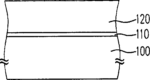
[0035] Please refer to Figure 1A , forming a dielectric layer 120 on the substrate 100 . The material of the dielectric layer 120 is, for example, a low dielectric constant material with a dielectric constant lower than 4, such as fluorine doped glass (FSG) or carbon doped glass (Si—O—C). Usually, before forming the dielectric layer 120 , there is already a capping layer 110 on the substrate 100 , the material of which is eg silicon nitride or silicon oxynitride.

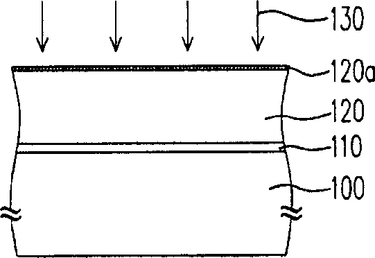
[0036] Please refer to Figure 1B After the dielectric layer 120 is formed, a processing step 130 is performed to reduce the doping concentration of the upper surface layer 120 a of the dielectric layer 120 . The processing step 130 is, for example, a plasma processing procedure, so that the doping concentration of the dielectric layer 120 at the upper...


PUM

PropertyMeasurementUnit
Thicknessaaaaaaaaaa

Abstract

The forming method for a stack structure of mosaic metal comprises: forming a doped dielectric layer on the substrate, treating the layer to make the doping concentration on top less than other; then, forming a metal hard mask layer on top. This invention can reduce the reaction of doped material and mask layer.

Description

technical field [0001] The present invention relates to a manufacturing method of a semiconductor element, in particular to a stack structure of a metal-containing hard mask layer for damascene, its forming method, and a corresponding damascene process, which can reduce the number of metal hard masks and other reaction between dopants in the underlying dielectric layer. Background technique [0002] With the advancement of semiconductor technology, the size of semiconductor elements is also continuously reduced, and enters the field of Deep Sub-Micron. When the integration of integrated circuits increases, the surface of the chip cannot provide enough area to make the required interconnection (Interconnect). Design becomes the way VLSI technology must adopt. [0003] In the process of multilayer metal interconnection, a thicker photoresist layer is generally required to avoid excessive consumption of the photoresist layer during the etching process of the dielectric layer....

Claims


Application Information

Patent Timeline
IPC IPC(8): H01L21/32H01L21/768
Inventor 林经祥刘志建
Owner UNITED MICROELECTRONICS CORP
Why Eureka
Try Eureka