Supercharge Your Innovation With Domain-Expert AI Agents!

Semiconductor device with low thermal expansion coefficient and use thereof

A thermal expansion coefficient, semiconductor technology, applied in the direction of semiconductor devices, semiconductor/solid-state device manufacturing, semiconductor/solid-state device components, etc., to achieve the effect of reducing structural distortion or deformation

Active Publication Date: 2007-01-10
TAIWAN SEMICON MFG CO LTD
View PDF0 Cites 1 Cited by
  • Summary
  • Abstract
  • Description
  • Claims
  • Application Information

AI Technical Summary

Problems solved by technology

[0010] The purpose of the present invention is to overcome the defects of existing semiconductor elements, and provide a semiconductor element with a low thermal expansion coefficient base material and its application of a new structure. The technical problem to be solved is to reduce the surface of the base material The structure distortion or deformation caused by heat will lead to the failure of semiconductor elements, which is more suitable for practical use and has industrial utilization value

Method used


Image

  • Semiconductor device with low thermal expansion coefficient and use thereof
  • Semiconductor device with low thermal expansion coefficient and use thereof
  • Semiconductor device with low thermal expansion coefficient and use thereof

Examples


Embodiment Construction

[0046] In order to further illustrate the technical means and effects adopted by the present invention to achieve the predetermined purpose of the invention, the following describes the specific implementation and structure of the semiconductor element with a low thermal expansion coefficient substrate according to the present invention with reference to the accompanying drawings and preferred embodiments. , features and their effects are described in detail below.

[0047] For clarity of illustration, elements in the figures are not drawn to scale. In different figures, the reference numerals of elements may be repeated to designate corresponding or similar elements.

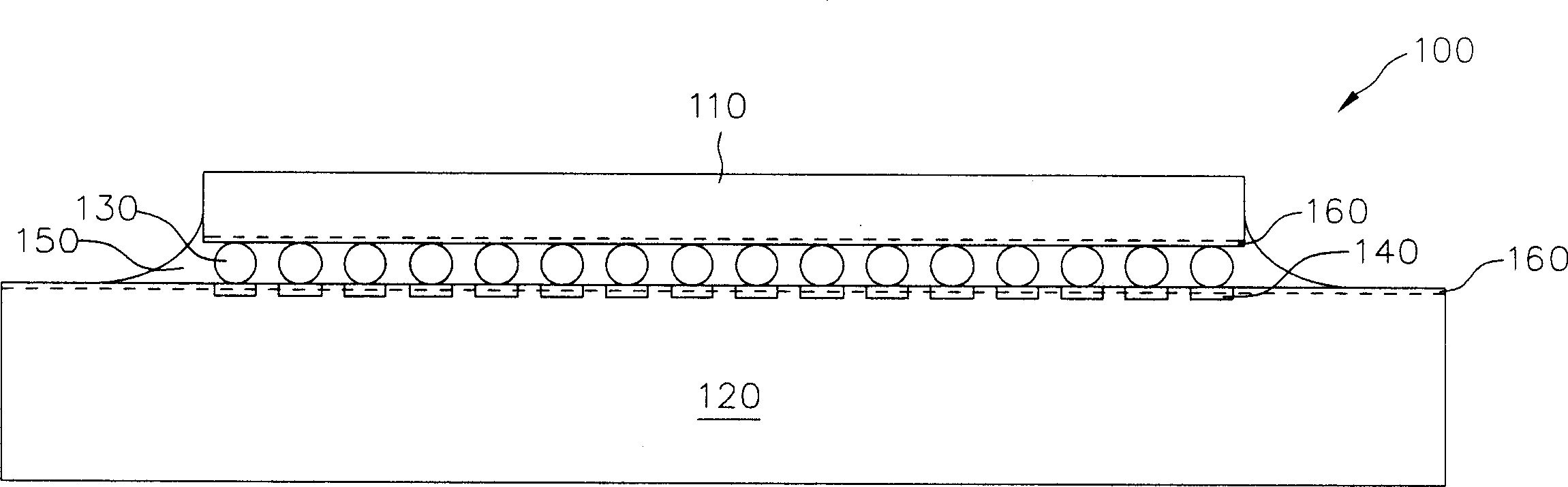
[0048] see figure 1 As shown, it is a schematic structural diagram of a semiconductor package device 100 according to a preferred embodiment of the present invention. Specifically, the semiconductor package device 100 includes an integrated circuit chip 110, wherein the integrated circuit chip 110 includes a ...


PUM


Abstract

The invention relates to a semiconductor device with low thermal expansion coefficient and use thereof, wherein the semiconductor device comprises an integrated circuit chip having at least one coupling component formed on an exterior surface thereof. Also, the device includes a package substrate having a mounting surface that are configured to receive plurality of bonding pads of at least one coupling component. In such embodiments, the package substrate is selected or manufactured such that it has a coefficient of thermal expansion in a direction perpendicular to its mounting surface that is less than approximately twice a coefficient of thermal expansion along a plane parallel to its mounting surface.

Description

technical field [0001] The present invention relates to a process technology of a semiconductor element and its application, in particular to a low coefficient of thermal expansion (CTE) substrate suitable for a low dielectric coefficient flip chip (Flip Chip) semiconductor package element. Background technique [0002] Integrated circuit chip packaging is one of the most important process steps in the integrated circuit chip manufacturing process, and has a considerable impact on the cost, performance and reliability of the overall device. When semiconductor components achieve a high degree of integration, packaging technology becomes critical. Since the packaging of integrated circuit chips accounts for a considerable part of the cost of manufacturing semiconductor devices, packaging failures can cause costly process yield drop problems. [0003] The continuous decrease in the feature size of semiconductor devices will lead to a substantial increase in the density of semi...

Claims


Application Information

Patent Timeline
Patent Type & Authority Applications(China)
IPC IPC(8): H01L23/488H01L23/50H01L23/373
CPCH01L23/15H01L21/563H01L2924/01037H01L2924/01068H01L2224/16H05K1/0271H01L2924/01019H01L2924/01322H05K3/4602H01L23/3128H05K2201/068H05K2201/10674H01L23/3735H01L23/14H01L2224/13116H01L2224/16227H01L2224/32225H01L2224/73204H01L2224/81805H01L2224/92125H01L2224/16225H01L2924/00
Inventor 卢思维李新辉李建勋李明机
Owner TAIWAN SEMICON MFG CO LTD
Features
  • R&D
  • Intellectual Property
  • Life Sciences
  • Materials
  • Tech Scout
  • Unparalleled Data Quality
  • Higher Quality Content
  • 60% Fewer Hallucinations
Learn More