Infrared imaging element
An imaging element, infrared technology, applied in electrical elements, pyroelectric devices, image communication, etc., can solve the problems that hinder the miniaturization and cost reduction of infrared detectors
- Summary
- Abstract
- Description
- Claims
- Application Information
AI Technical Summary
Problems solved by technology
Method used
Image
Examples
Embodiment approach 1
[0065] Hereinafter, an embodiment of the present invention will be described by taking an infrared camera as an example.
[0066] The infrared camera of the present embodiment is an infrared camera provided with the infrared imaging element of the present invention, and makes infrared rays emitted from a subject enter the infrared imaging element via an optical system including a lens etc. Take a video.
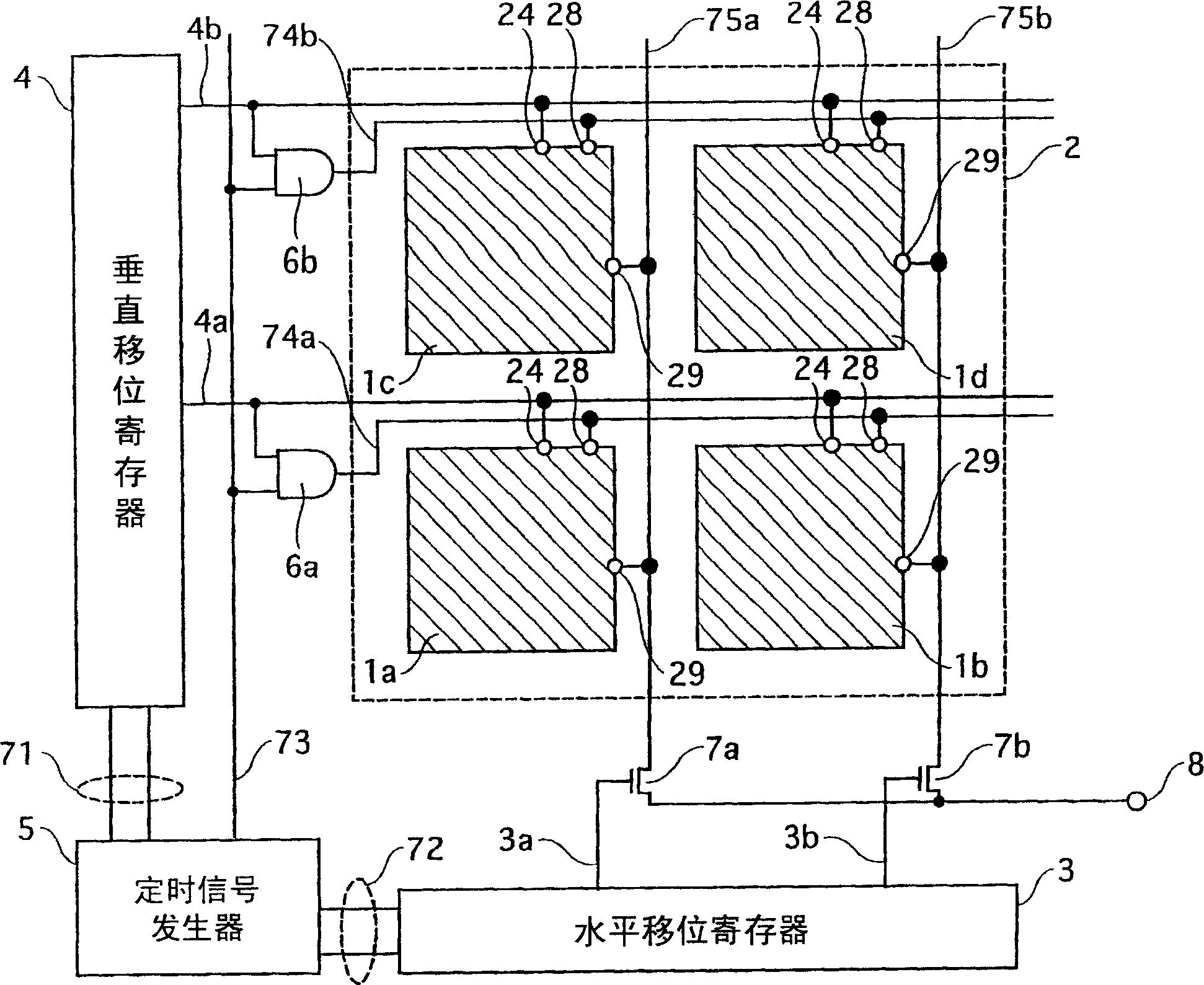
[0067] figure 1 It is a diagram showing the main circuit configuration of the infrared imaging device according to the embodiment.
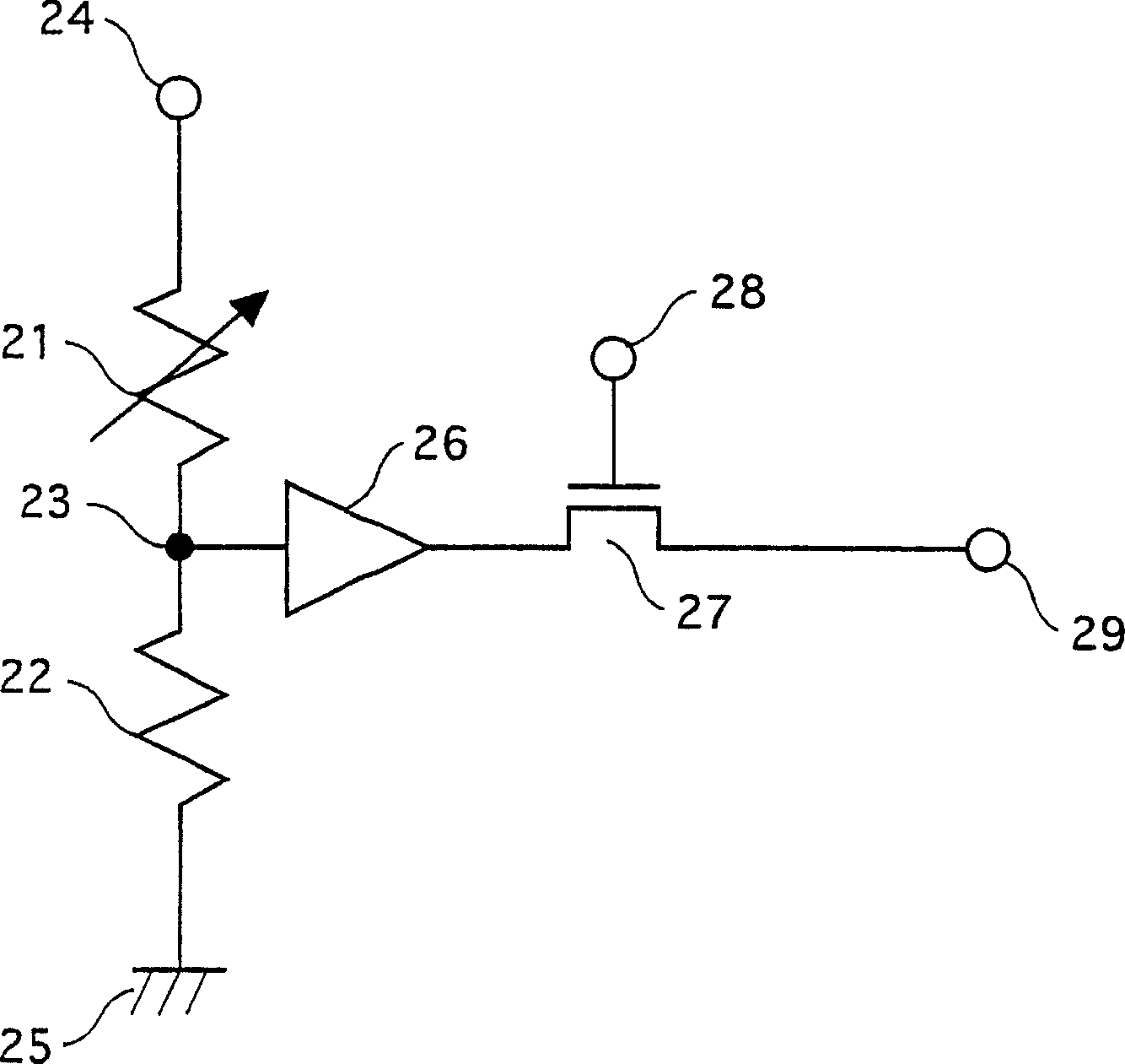
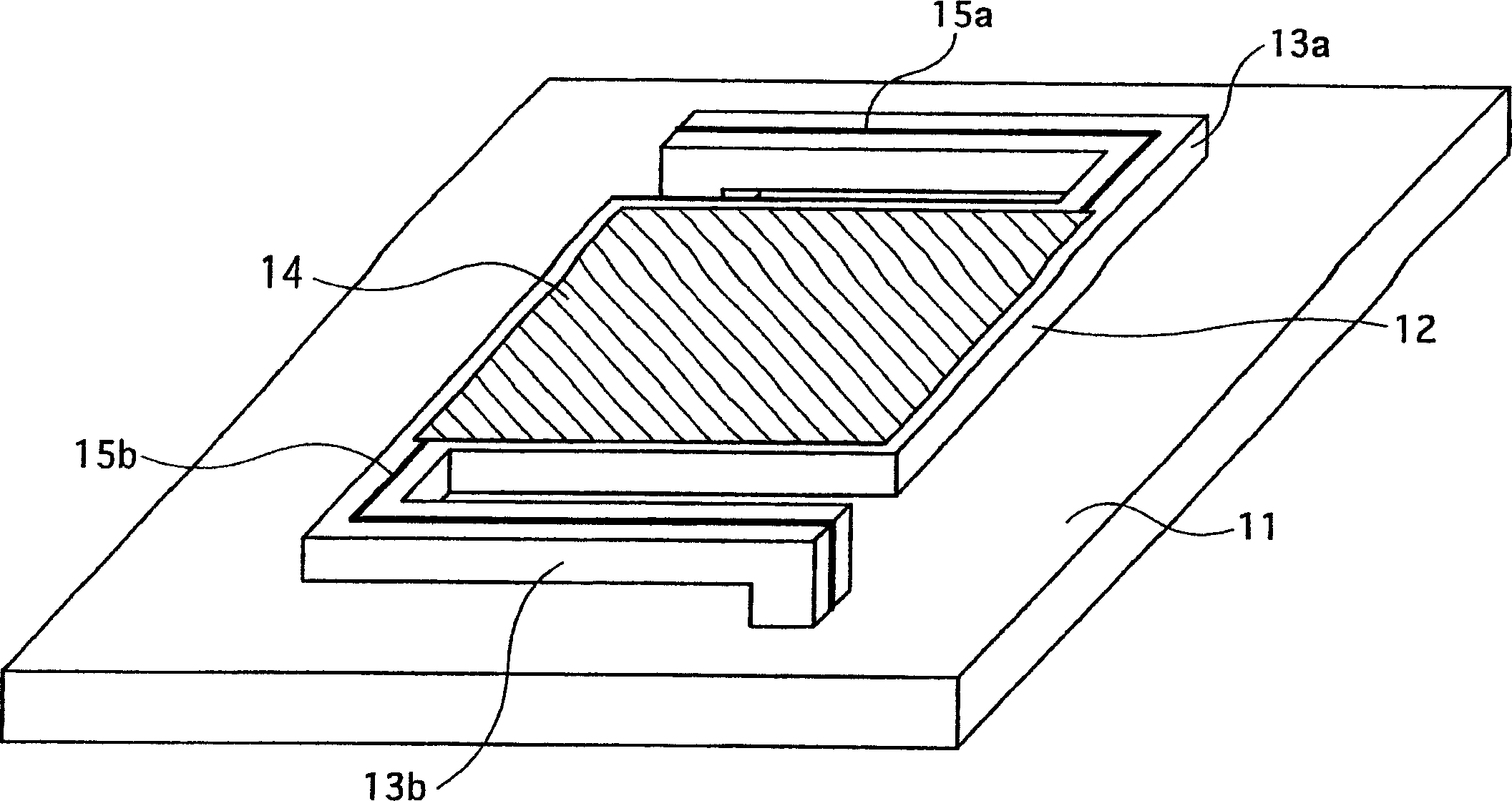
[0068] The infrared imaging element includes a plurality of infrared detectors (1a, 1b, 1c, 1d) and a detection circuit for detecting a change in resistivity of a thermistor of each infrared detector, which are formed on a common semiconductor substrate. Here, the detection circuit includes: a horizontal shift register 3 , a vertical shift register 4 , a timing signal generator 5 , wiring, and the like. In addition, for the convenience of des...
Embodiment approach 2
[0100] The infrared camera of this embodiment has substantially the same configuration as the infrared camera of Embodiment 1, but differs in the selection of the material of the thermistor.
[0101] In Embodiment 2, as the thermistor 14, La 1-X B X TiO 3 (B is an alkaline earth metal).
[0102] Perovskite LaTiO 3 It is a representative Mott insulator in which electrons occupy 3d orbitals. This Mott transition is caused by the 3d electrons of Ti, so the amount of electrons supplied to the 3d orbitals, the energy band structure of the 3d orbitals, and the like are factors that determine the phase transition temperature.
[0103] Thus, like La 1-X B X TiO 3 Like, through the LaTiO 3 Substituting part of the trivalent rare earth metal La with the divalent alkaline earth metal Ca can reduce the supply of electrons to the 3d orbital (equivalent to doping holes), thereby changing the phase transition temperature.
[0104] In addition, this replacement can be realized by mix...
Embodiment approach 3
[0112] The infrared camera of this embodiment has substantially the same configuration as that of the infrared camera of Embodiment 1, but differs in the selection of the material of the thermistor.
[0113] In Embodiment 3, RNiO 3 (R is yttrium or a rare earth metal).
[0114]It is well known that metal-insulator phase transitions also occur outside of perovskite-structured manganese oxides. As its representative is RNiO 3 Nickel oxides with the described perovskite structure.
[0115] nO 3 It is a typical Mott insulator in which the phase transition temperature of the metal-insulator phase transition varies depending on the type of R.
[0116] The reason why the phase transition temperature varies depending on the type of R is that the transfer energy of 3d electrons between adjacent Ni varies depending on the ion radius of R. Since the phase transition temperature is determined by the balance between the Coulomb repulsion energy between electrons and the transfer energ...
PUM
 Abstract
Description
Claims
Application Information


