Differential driving circuit and electronic equipment including the same

A differential drive and circuit technology, applied in differential amplifiers, logic circuit connections/interface layouts, amplifiers with semiconductor devices/discharge tubes, etc., to achieve high drive capabilities, reduce EMI problems, and solve oscillation problems

Inactive Publication Date: 2007-02-21
THINE ELECTRONICS
View PDF2 Cites 12 Cited by
  • Summary
  • Abstract
  • Description
  • Claims
  • Application Information

AI Technical Summary

Problems solved by technology

Accordingly, it is an object of the present invention to provide a differential driving circuit for low-voltage differential signals and electronic equipment including such a circuit, in which the circuit area and current can be reduced by eliminating or reducing the number of differential amplifiers. consumes and can solve the problem of oscillation caused by noise, and by making the common mode level stable, the occurrence of EMI problems can be reduced and high drive capability can be provided

Method used


Image

  • Differential driving circuit and electronic equipment including the same
  • Differential driving circuit and electronic equipment including the same
  • Differential driving circuit and electronic equipment including the same

Examples


no. 1 example

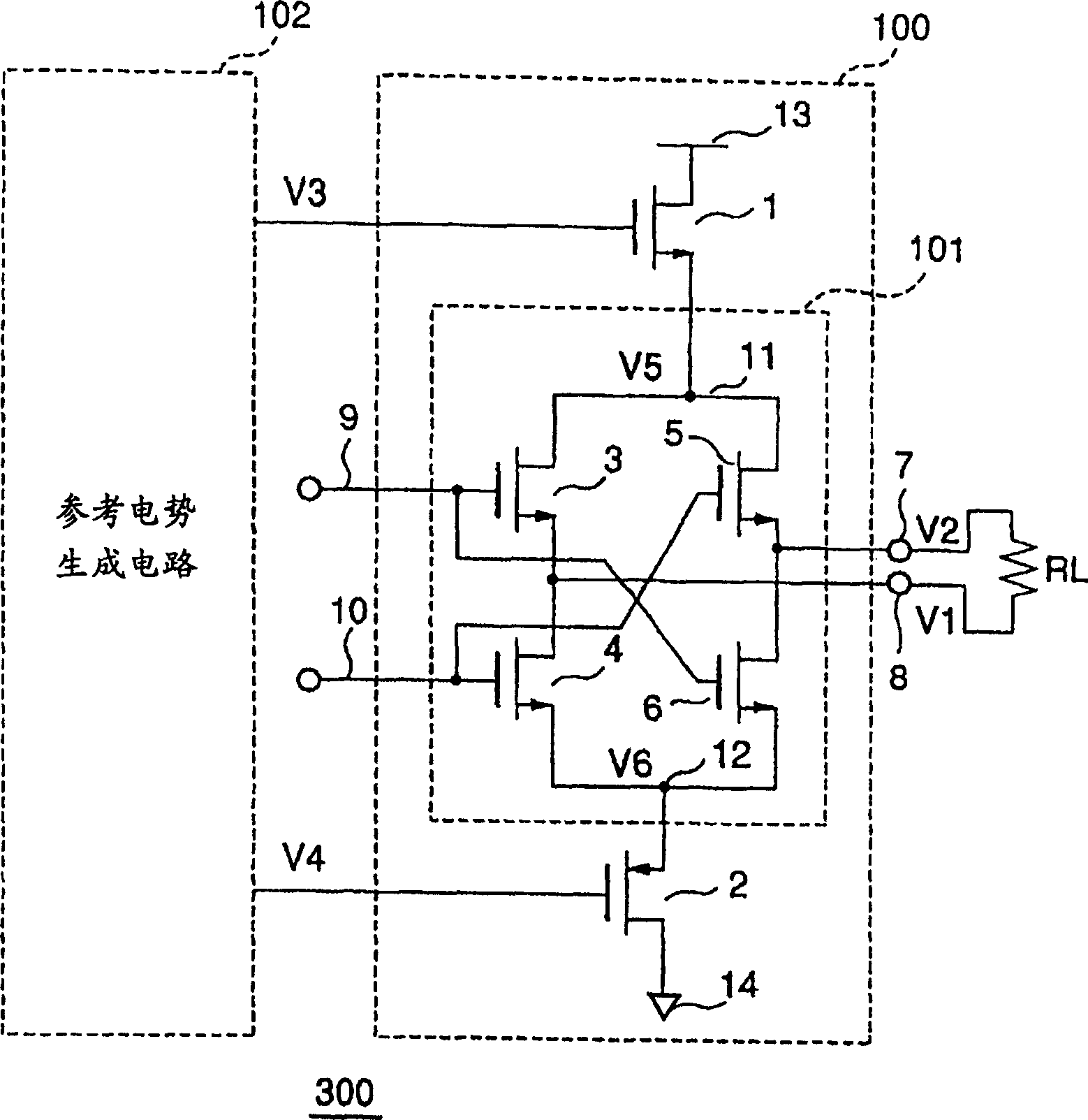
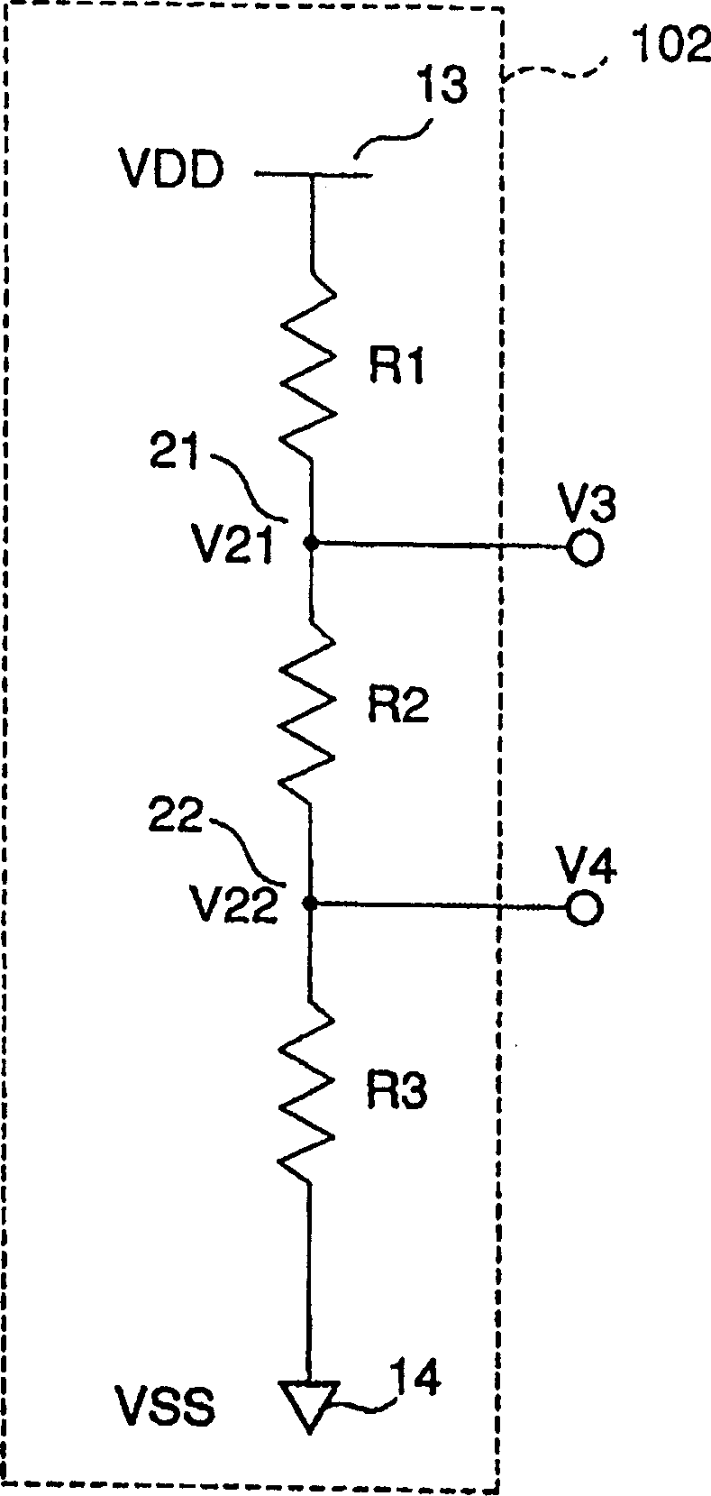
[0099] The following will use figure 1 A first embodiment of a differential drive circuit for low-voltage differential signals according to the present invention will be described. figure 1 is a circuit block diagram illustrating the configuration of the differential drive circuit for low voltage differential signals of the present invention. The differential drive circuit 300 for low-voltage differential signals of the present invention includes an output circuit 100 and a reference voltage generation circuit 102 complying with the LVDS interface standard (IEEE P1596, 3).

[0100] The output circuit 100 includes: a switch circuit 101 that receives a differential signal input to a terminating resistor RL and outputs a current signal to the terminating resistor RL; a PMOS (P-channel metal oxide semiconductor) transistor 2 that has one end connected to a low A power supply potential 14 on the potential side and the other end is connected to the node 12 in the switch circuit 101...

no. 2 example

[0110] The following will be done by using Image 6 A second embodiment of the differential drive circuit for low-voltage differential signals according to the present invention will be described. Image 6 is a circuit block diagram describing the configuration of the high output differential drive circuit of the present invention. The differential drive circuit 300 for low-voltage differential signals of the present invention includes an output circuit 100 , a strengthening circuit 300 and a bias circuit (not shown) for these circuits, such as a reference potential generating circuit 102 .

[0111] The output circuit 100 is figure 1 circuit described in . In the booster circuit 400, the drain of the PMOS transistor 61 is connected to a node 71 in a switch circuit for a booster circuit including a MOS transistor to which a differential signal different from the signal input to the drive circuit 100 is input. , and the switching circuit outputs a current signal. The source ...


PUM


Abstract

A differential driving circuit used for low voltage differential signals and an electronic device incorporating the same are provided wherein no differential amplifiers are used or the number of differential amplifiers are reduced, thereby reducing the circuit area and the current consumption and further solving the problem of oscillation caused by noise, while a high driving performance is achieved. There are included a switch circuit, an output circuit and a reference potential generating circuit. The switch circuit, which comprises MOS transistors, receives differential signals and outputs current signals. The output circuit comprises an NMOS transistor, an end of which is connected to the power supply potential of a higher potential side, the other end of which is connected to a node of the switch circuit and which acts as a source follower, and an PMOS transistor, an end of which is connected to the power supply potential of a lower potential side, the other end of which is connected to the other node of the switch circuit and which acts as a source follower. The reference potential generating circuit supplies reference potentials to the respective gates of the PMOS and NMOS transistors. The reference potential generating circuit includes a potential varying means that varies the differential potentials with an offset potential kept constant. Further, there is included an emphasis circuit for the output circuit.

Description

technical field [0001] The present invention relates to a differential drive circuit for an LVDS (Low Voltage Differential Signaling) interface that transmits a signal by changing the flow direction of current in a pair of resistor-terminated differential transmission lines, and a differential drive circuit including the same Electronic equipment. Background technique [0002] As for the differential driving circuit for the LVDS interface, there is known a scheme described in Patent Document 1 which will be listed below. The drive circuit proposed here employs a configuration in which the differential voltage is varied while the compensation potential is kept constant by using three differential amplifiers. Therefore, there are problems in that the circuit becomes complicated, the circuit area and the total current consumption increase, and there is a high possibility that the two differential amplifiers driving the transistors of the final stage will cause oscillation, whi...

Claims


Application Information

Patent Timeline
Patent Type & Authority Applications(China)
IPC IPC(8): H03K19/0185H03F3/45
CPCH03F2203/45318H03F2203/45466H03F3/45179H04L25/028H03F3/45183H03F3/505H04L25/0272
Inventor 三浦贤冈村淳一小泽诚一
Owner THINE ELECTRONICS
Why Eureka
Try Eureka