Solid-state imagine device, line sensor, optical sensor, and method for operating solid-state imaging device

A technology of a solid-state imaging device and a working method, which is applied to radiation control devices, image communication, television, etc., can solve the problems of inability to match two images, low sensitivity, and difficulty in high sensitivity.

Active Publication Date: 2007-03-07
TOHOKU UNIV
View PDF4 Cites 15 Cited by
  • Summary
  • Abstract
  • Description
  • Claims
  • Application Information

AI Technical Summary

Problems solved by technology

[0014] However, in the methods described in Patent Documents 1, 2, and 3 and Non-Patent Document 2 or the method of capturing images twice with different exposure times, it is necessary to perform the imaging of the low-illuminance side and the imaging of the high-illuminance side at different times. camera, so if you shoot a movie, there will be a shift in the camera image corresponding to the two illuminances, and there is a problem that the two images cannot be matched.
[0015] In addition, in the methods described in Patent Document 4 and Non-Patent Document 3, it is possible to realize a wide dynamic range for imaging on the high-illuminance side, but it has low sensitivity and low S / N for imaging on the low-illuminance side. ratio, the image quality cannot be improved
[0016] As mentioned above, in image sensors such as CMOS image sensors, it is difficult to achieve a wide dynamic range while maintaining high sensitivity and high S / N ratio
[0017] In addition, the fact described above is not limited to image sensors, and it is also difficult to achieve a wide range while maintaining high sensitivity and a high S / N ratio as a line sensor in which pixels are arranged in a straight line or a photosensor that does not have a plurality of pixels. Dynamic Range

Method used


Image

  • Solid-state imagine device, line sensor, optical sensor, and method for operating solid-state imaging device
  • Solid-state imagine device, line sensor, optical sensor, and method for operating solid-state imaging device
  • Solid-state imagine device, line sensor, optical sensor, and method for operating solid-state imaging device

Examples


Embodiment approach 1

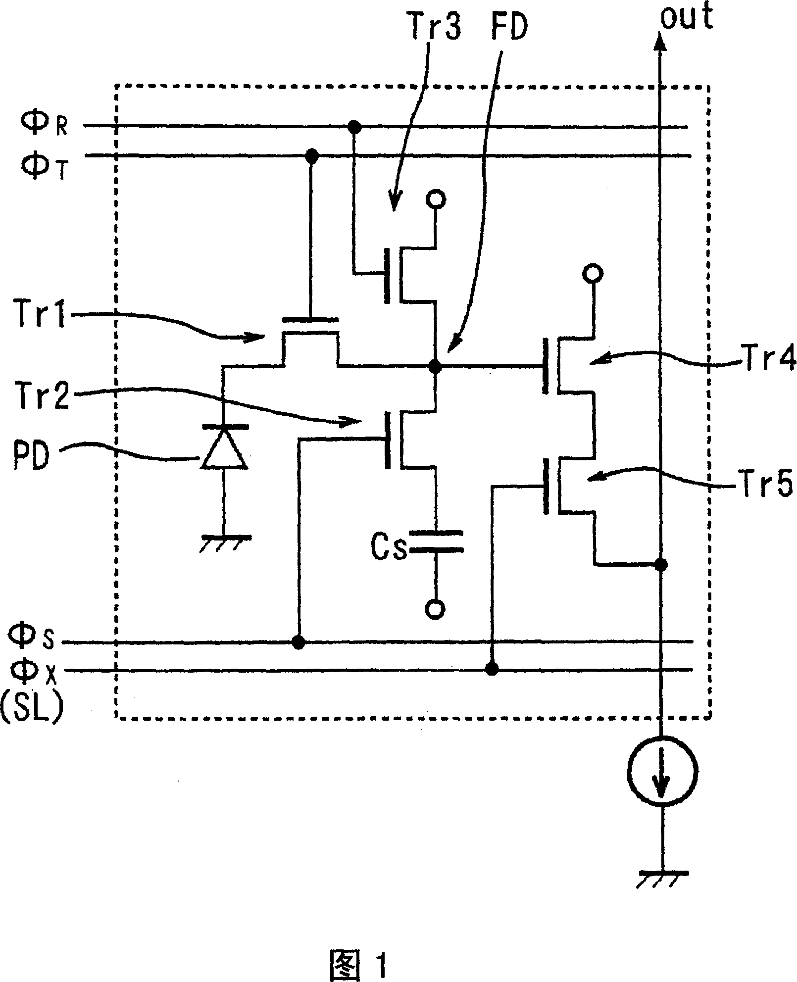
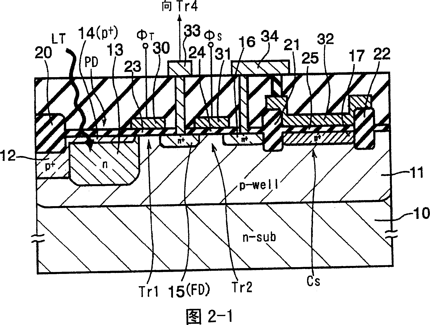
[0143] The solid-state imaging device of this embodiment is a CMOS image sensor, and FIG. 1 is an equivalent circuit diagram of one pixel.

[0144] Each pixel consists of a photodiode PD that receives light and generates photocharges, a transfer transistor Tr1 that transfers photocharges from the photodiode PD, a floating region FD that transfers photocharges through the transfer transistor Tr1, and accumulates photocharges from the photodiodes during an accumulation operation. The overflow photocharge storage capacitor element C S , The floating area FD and the storage capacitor element C S The storage transistor Tr2 that is combined or divided by the potential of the floating region FD, the reset transistor Tr3 that is formed in connection with the floating region FD and used to discharge the photocharges in the floating region FD, and the amplifier that transforms the photocharges in the floating region FD into a voltage signal The transistor Tr4 and the selection transist...

Embodiment approach 2

[0219] This embodiment is a form in which the circuit configuration of the pixel of the CMOS image sensor in the first embodiment is modified.

[0220] FIG. 9-1 is an equivalent circuit diagram of one pixel of an example of the CMOS image sensor of this embodiment. It is substantially the same as the equivalent circuit diagram of FIG. 1, but the connection between the amplification transistor Tr4 and the selection transistor Tr5 is different. The selection transistor Tr5 is arranged on the upper side of the amplification transistor Tr4, and the output of the amplification transistor Tr4 is connected to the output line out. .

[0221] By connecting in this way, the gain of the amplifier of the amplifier transistor Tr4 can be increased.

[0222] 9-2 is an equivalent circuit diagram of one pixel of another example of the CMOS image sensor of this embodiment. It is substantially the same as the equivalent circuit diagram of FIG. 1, but for the five transistors including the tran...

Embodiment approach 3

[0227] The solid-state imaging device of this embodiment is a CCD image sensor.

[0228] FIG. 10-1 is an equivalent circuit diagram of one pixel of an example of the CCD image sensor of this embodiment.

[0229] φ V1 and φ V2 The first charge-coupled transfer line CCD1 and the second charge-coupled transfer line CCD2 of the 2-phase drive are arranged to extend in the vertical direction, the photodiode PD is directly connected to the first charge-coupled transfer line CCD1, and is connected to the second charge-coupled transfer line via the transfer transistor Tr1 Forwarding route to CCD2 connection.

[0230] Here, the second charge-coupled transfer line CCD2 functions as a storage capacitor element C that accumulates photocharges overflowing from the photodiode PD when the photodiode PD is saturated. S kick in.

[0231] In the CCD image sensor of the above-mentioned structure, the signal before saturation on the low-illuminance side is transferred through the first charge-...


PUM


Abstract

A solid-state imaging device having a widened dynamic range while maintaining a high sensitivity and a high S/N ratio, a line sensor, an optical sensor, and a method for operating a solid-state imaging device adopted so as to widen the dynamic range of the solid-state imaging device while maintaining a high sensitivity and a high S/N ratio are disclosed. The solid-state imaging device is composed of an array of integrated pixels each of which comprises a photodiode (PD) for generating optical charges on receiving light, a transfer transistor (Tr1) for transferring the optical charges, and a storage capacitive element (Cs) connected to the photodiode (PD) at least through the transfer transistor (Tr1) and serving to store the optical charges overflowing from the photodiode (PD) at least through the transfer transistor (Tr1) during storage operation.

Description

technical field [0001] The present invention relates to a solid-state imaging device, a line sensor, an optical sensor and a working method of the solid-state imaging device, in particular to a CMOS or CCD type solid-state imaging device, a line sensor, an optical sensor and a working method of the solid-state imaging device. Background technique [0002] Image input image sensors such as CMOS (Complementary Metal-Oxide-Semiconductor) image sensors and CCD (Charge Coupled Device) image sensors need to be expanded in applications such as digital cameras and mobile phones with cameras while improving their characteristics. [0003] Further characteristic improvements are desired for the image sensor, one of which is to expand the dynamic range. [0004] The dynamic range of conventionally used image sensors has been limited to, for example, 3 to 4 digits (60 to 80 dB), but the current situation is as big as 5 to 6 digits (100 to 120 dB) of the naked eye or silver salt thin fil...

Claims


Application Information

Patent Timeline
Patent Type & Authority Applications(China)
IPC IPC(8): H01L27/146H04N5/335H04N5/3745H04N5/378
CPCH04N5/3559H04N5/37452H04N5/374H04N25/59H04N25/771H04N25/76
Inventor 须川成利
Owner TOHOKU UNIV
Why Eureka
Try Eureka