

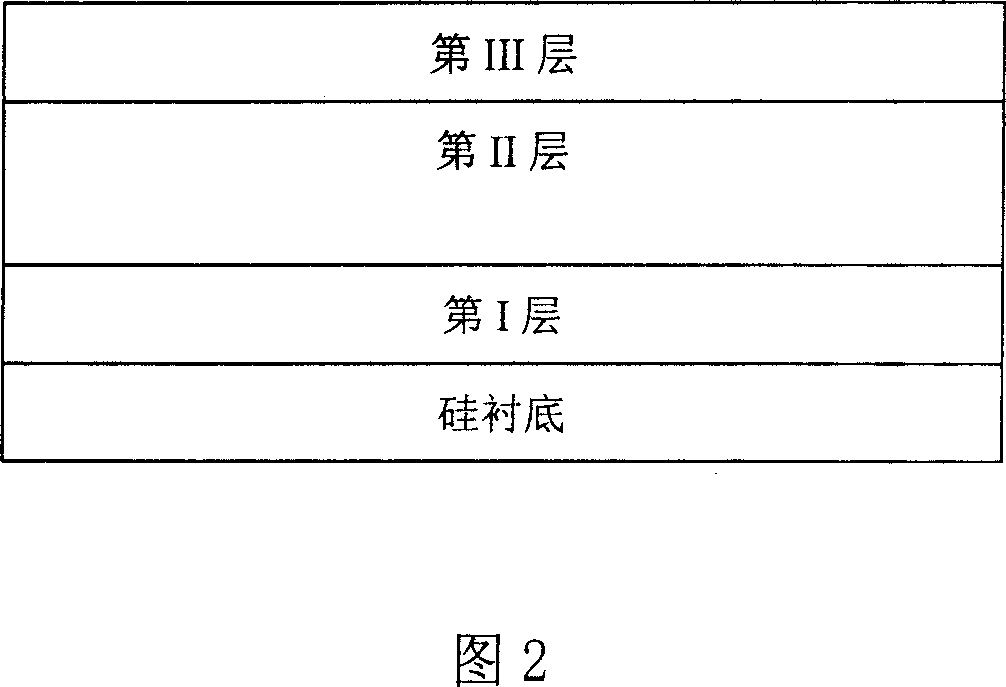
Method for preparing thickness controllable trilayer type diamond membrane
A technology of diamond thin film and thin film, which is applied in the direction of coating, metal material coating process, gaseous chemical plating, etc., to achieve the effect of large thickness
- Summary
- Abstract
- Description
- Claims
- Application Information
AI Technical Summary
Problems solved by technology
Method used
Image

Examples
Embodiment 1
[0039] Process and steps in the present embodiment are as follows:
[0040] 1. Pretreatment of silicon wafer substrate: put a 10×10mm silicon wafer in HF solution for 5 minutes to remove the surface oxide layer of the silicon wafer, and then manually grind it with ultra-fine diamond powder with a particle size of 100nm for 15 minutes to make Very fine uniform scratches are formed on the surface, and finally the surface is cleaned repeatedly with acetone and deionized water respectively;
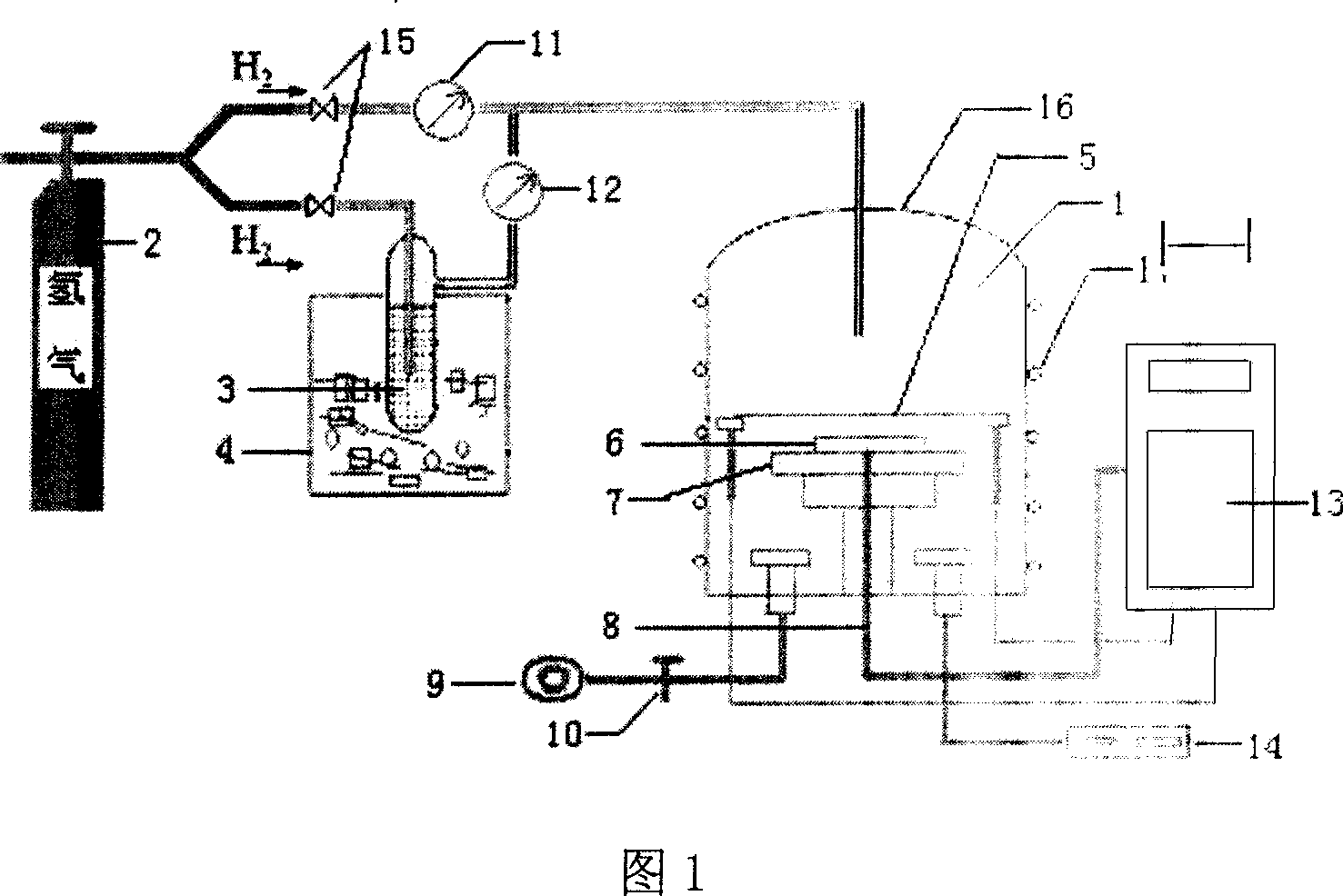
[0041] 2. Utilize the traditional and existing hot wire chemical vapor deposition experimental device for three-stage three-layer deposition of diamond film (see Figure 1):
[0042] (1) Deposition of the first layer of diamond film in the first stage: This is the deposition of the first layer of diamond film on the treated silicon wafer substrate placed on the sample stage, and it is also the crystal bottom layer of the entire three-layer film ;The silicon wafer substrate is placed 8mm away ...
PUM
 Abstract
Description
Claims
Application Information