Phase transformation memory storing unit and producing method thereof

A technology of phase-change memory and storage unit, applied in the field of microelectronics, which can solve the problems of reducing operating current, large device operating current, and high power consumption, and achieve the effect of reducing contact area, small contact area, and reducing power consumption

Active Publication Date: 2007-03-21
SHANGHAI INST OF MICROSYSTEM & INFORMATION TECH CHINESE ACAD OF SCI
View PDF0 Cites 20 Cited by
  • Summary
  • Abstract
  • Description
  • Claims
  • Application Information

AI Technical Summary

Problems solved by technology

At the beginning of 2006, Samsung has prepared a 256M C-RAM memory test sample using a 0.12μm process, but the operating current of the device is still relatively large, the power consumption is relatively high, and the stability of the device needs to be further improved
In order to reduce the contact area between the heating electrode and the phase change material, South Korea’s Samsung Company has adopted a ring-shaped heating electrode structure, which can adjust the contact area by controlling the wall thickness of the ring-shaped heating electrode, which can greatly reduce the operating current, but they The ring-shaped heating electrode structure is not hollow, but filled with some kind of insulating material. Such a structure cannot make the phase change material confined in the heating electrode [Jpn.J.Appl.Phys., 2006, 45, 3233]

Method used


Image

  • Phase transformation memory storing unit and producing method thereof
  • Phase transformation memory storing unit and producing method thereof
  • Phase transformation memory storing unit and producing method thereof

Examples


Embodiment 1

[0034] A specific preparation process of a phase change memory storage unit is as follows:

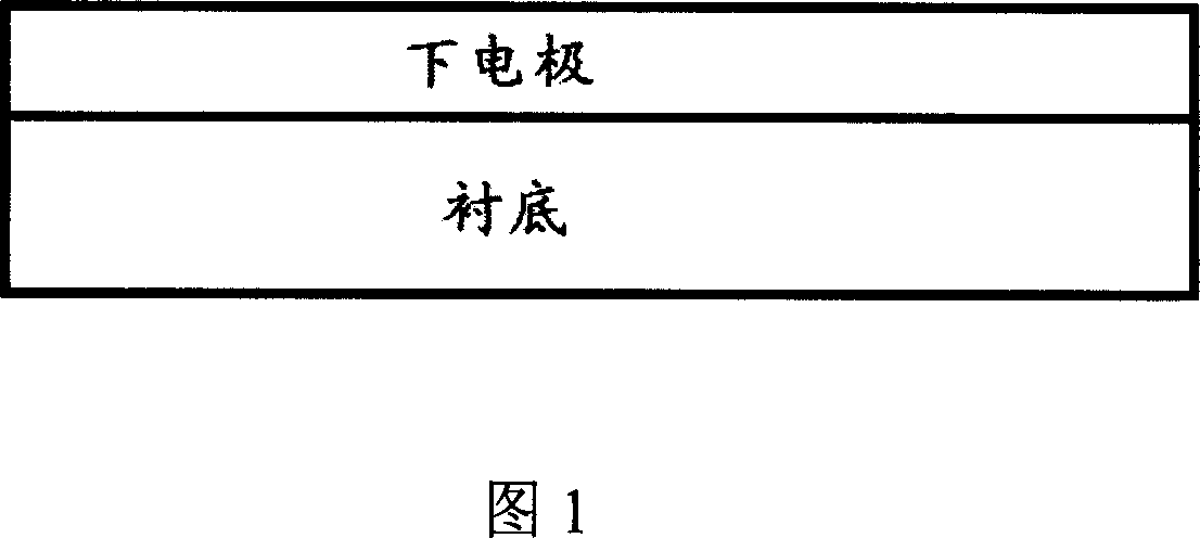
[0035] 1) covered with SiO 2 A layer of Al lower electrode layer was prepared by DC magnetron sputtering on the silicon substrate, and the SiO on the silicon substrate 2 Prepared by thermal oxidation method, SiO 2 The thickness of the material is 1000 nm. The process parameters for preparing Al electrodes are: the background pressure is 2×10 -4 Pa, the Ar gas pressure during sputtering is 0.2Pa, the sputtering power is 200W, the substrate temperature is 25°C, and the film thickness is 400nm. (figure 1)

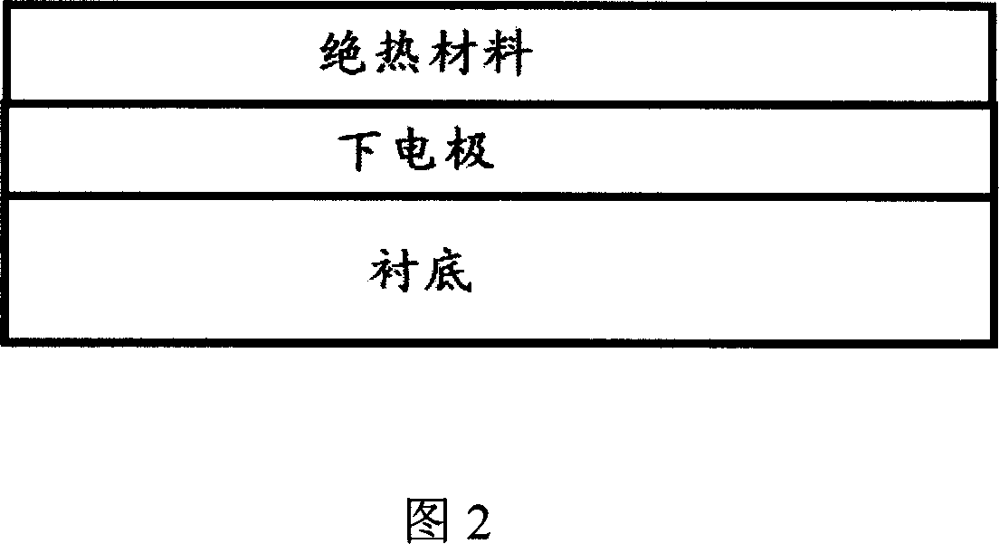
[0036] 2) Preparation of SiO on Al electrode 2 The thermal insulation material layer is a chemical vapor deposition method, and the thickness of the film is 500nm. (figure 2)

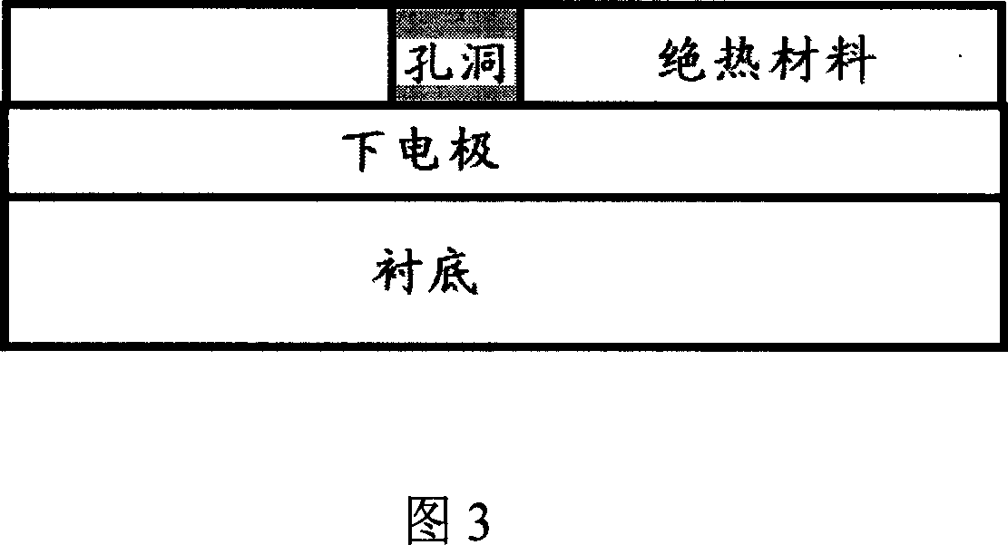
[0037] 3) Using 0.18μm standard process on SiO 2 Holes are prepared in the heat insulating material layer, and the diameter of the holes is 260 nm. (image 3)

[0038] 4) Use chemical vapor deposition t...

Embodiment 2

[0051] The W columnar electrode in Embodiment 1 is changed to TiN, and the rest is similar to Embodiment 1.

Embodiment 3

[0053] The Ge of embodiment 1 and embodiment 2 2 Sb 2 Te 5 Phase change film changed to Si 2 Sb 2 Te 5 Phase change thin film, all the other are similar to embodiment 1 and embodiment 2.


PUM

PropertyMeasurementUnit
diameteraaaaaaaaaa
thicknessaaaaaaaaaa
diameteraaaaaaaaaa

Abstract

This invention relates to a phase-transformation storage unit and its preparation method charactering in covering a lower electrode layer on the substrate, covering a heat insulation material layer with holes on the lower electrode layer, and the holes contain a hollow column heating electrode material structure conducting to the lower electrode, a heat insulation material layer covers the column heating electrode and contains holes matched to the heating electrode and an inverse phase-transformation material layer covered by a heat insulation material layer with holes is contained in the electrode holes and the holes of the insulation material layer, and the upper electrode material is filled in the holes of the heat insulation layer conducting to the phase-transformation material, which limits the phase-transformation material in the holes in the hollow post and the insulation material to keep the phase-transformation material to be transformed first at the environment high temperature and high pressure when electric pulse operates a storage unit.

Description

technical field [0001] The invention relates to a storage unit structure of a phase-change memory and a preparation method thereof, in particular to a hollow column-shaped heating electrode prepared by micro-nano processing technology, and a phase-change material is filled in the hollow column to utilize the electric pulse action The change of temperature and pressure in the lower hollow column induces the phase change of the phase change material, thereby realizing the low voltage, low power consumption and high speed functions of the phase change memory unit. The invention belongs to the technical field of microelectronics. Background technique [0002] Phase-change memory (C-RAM, Chalcogenide-Random Access Memory) technology is based on Ovshinsky in the late 1960s (Phys. Rev. Lett., 21, 1450-1453, 1968) and early 1970s (Appl. Phys. Lett. , 18, 254-257, 1971) put forward the idea that the phase-change thin film can be applied to the phase-change storage medium. The chara...

Claims


Application Information

Patent Timeline
Patent Type & Authority Applications(China)
IPC IPC(8): H01L45/00H01L27/24G11C11/56
Inventor 宋志棠刘波封松林陈邦明
Owner SHANGHAI INST OF MICROSYSTEM & INFORMATION TECH CHINESE ACAD OF SCI
Why Eureka
Try Eureka