Cathode flow field plate for self-breathing micro-proton exchange film fuel cell and producing method
A technology of proton exchange membrane and cathode flow field, which is applied to fuel cell components, solid electrolyte fuel cells, fuel cells, etc., can solve the problems of unsatisfactory battery performance and large battery contact resistance, and improve the effective utilization rate, The effect of improving battery performance and reducing contact resistance
- Summary
- Abstract
- Description
- Claims
- Application Information
AI Technical Summary
Problems solved by technology
Method used
Image
Examples
Embodiment 1
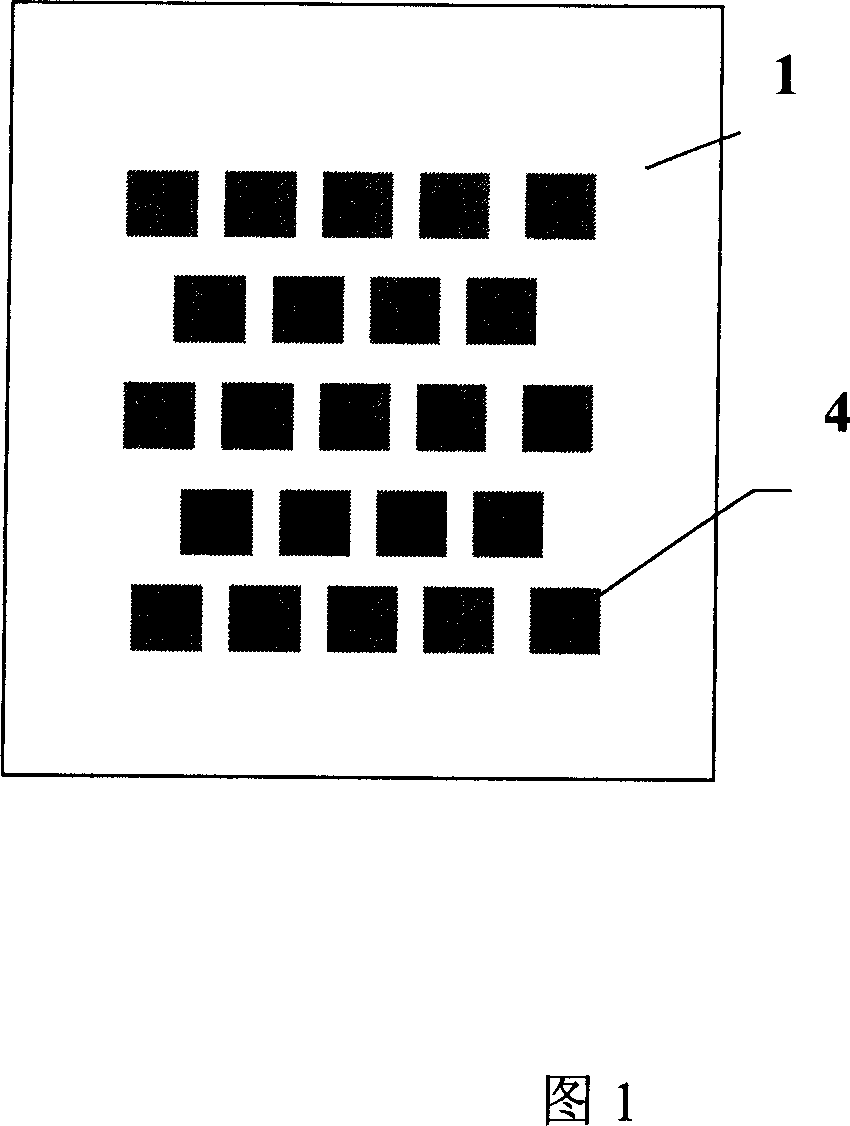
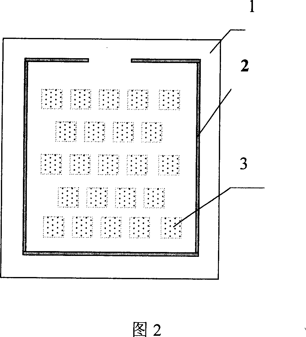
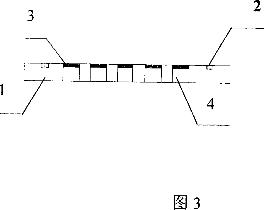
[0036]Select N(100) silicon wafers with a thickness of 350 μm and a resistivity of less than 15Ω·cm. According to the structure shown in Figure 1-3, both the front and back sides are dry-etched (DRIE method) to produce a cathode double-layer with an effective area of 1.2×1.2cm. Layer hollow flow field structure, the flow channel on the air side is of equal diameter, with a cross-sectional area of 300×300 μm, the layer thickness is 290 μm, and the duty ratio is 70%; the flow channel near the membrane electrode side is also of equal diameter, with a cross-sectional area of 11 μm×11 μm, and The ratio is 50%, and the thickness is 60 μm. Fig. 4 is the SEM image of the prepared cathode structure, wherein (a) is a photo of the structure near the flow channel on the air side, and (b) is an enlarged photo of the small hole structure corresponding to the back side of the air side flow channel (near the MEA side); Fig. 5 is a SEM photo of the cross-section of the structure inclined...
Embodiment 2
[0041] Select an N(100) silicon wafer with a thickness of 350 μm and a resistivity of less than 15Ω·cm, and adopt the same method as the manufacturing process steps (1)-(4) to form etching windows each with a size of 800 μm×800 μm on the front side of the silicon wafer , using dry etching (DRIE), controlling the etching time, so that a straight hole of equal diameter and 250 μm deep is formed; after cleaning, a thin layer of SiO on the back is removed 2 Finally, each etching window with a size of 100 μm×100 μm is exposed, and the silicon wafer is placed in a KOH solution with a concentration of 40 vol% at 50° C., and both sides are wet-etched simultaneously until the silicon substrate is penetrated. The formed double-layer flow field structure has macropores of equal diameter on the upper side and tapered holes on the lower side. The upper surface area is 800 μm×800 μm, the lower surface area is 730 μm×730 μm, the thickness of the macroporous layer is 300 μm, and the duty cycle...
Embodiment 3
[0043] Select an N(100) silicon wafer with a thickness of 300 μm and a resistivity of less than 15Ω·cm, and adopt the same method as the manufacturing process steps (1)-(4), and form a 1.5mm×1.5mm silicon wafer on the front surface of the silicon wafer. The corrosion window is wet-etched, that is, at 50°C, in a KOH solution with a concentration of 40vol%, and the etching time is controlled to form a tapered hole with a depth of 200 μm; after cleaning, a thin layer of SiO on the back is removed 2 Finally, each etching window with a size of 100 μm×100 μm is exposed, and the silicon wafer is placed in a 50° C., 40% (Vol%) KOH solution to continue etching until the silicon substrate is penetrated. The formed double-layer flow field structure, the upper surface area of the large hole is 1.5mm×1.5mm, the lower surface area is 1.15mm×1.15mm, the total thickness of the large hole layer is 250μm, and the duty ratio is 85%; the small hole The layer has a cone-shaped pore structure, th...
PUM
| Property | Measurement | Unit |
|---|---|---|
| thickness | aaaaa | aaaaa |
| thickness | aaaaa | aaaaa |
| electrical resistivity | aaaaa | aaaaa |
Abstract
Description
Claims
Application Information


