Semiconductor laser shaper

A shaping device and laser technology, applied in the field of lasers, can solve the problems of small adjustment tolerance of cylindrical lenses, difficult focal length processing, complex structure, etc., and achieve the effects of small light energy loss, convenient collimation and coupling, and small volume

Inactive Publication Date: 2007-03-21
西安飞秒光纤技术有限公司
View PDF1 Cites 11 Cited by
  • Summary
  • Abstract
  • Description
  • Claims
  • Application Information

AI Technical Summary

Problems solved by technology

[0006] At present, there are three types of beam shaping devices for semiconductor lasers. One is the cylindrical lens to collimate and shape the angle in the fast axis direction. The adjustment tolerance of the cylindrical lens is small, and it is difficult to process the focal length very small.
The other uses a single lens to collimate the output beam of the semiconductor laser. This semiconductor laser beam shaping device has a simple structure, convenience and economy, but the effect is poor, the degree of collimation is low, and the...

Method used


Image

  • Semiconductor laser shaper
  • Semiconductor laser shaper
  • Semiconductor laser shaper

Examples


Embodiment 1

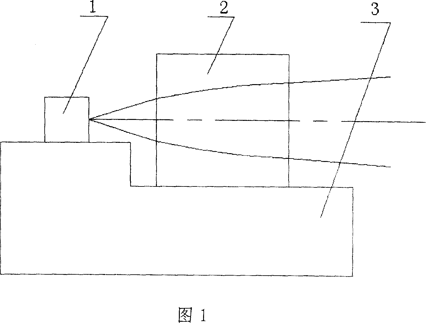
[0029] In FIG. 1 , the semiconductor laser shaping device of this embodiment is composed of a bracket 3 , a semiconductor laser 1 , and a one-dimensional gradient index lens 2 connected together.

[0030] A semiconductor laser 1 is fixedly installed on the bracket 3 , the model of the semiconductor laser 1 in this embodiment is QL65D5SA, the wavelength is 650nm, and its light emitting area is 5um×2um. On the bracket 3, the direction in which the semiconductor laser 1 emits the laser beam is placed horizontally and fixedly installed with a one-dimensional gradient refractive index lens 2. The one-dimensional gradient refractive index lens 2 is a rectangular flat plate lens, and this lens has gradient refraction only in the thickness direction of the lens. rate, the thickness of the one-dimensional gradient index lens 2 is 0.3mm, the length of the light is 1.5mm, the width is 2mm, and the focusing constant is 2.51. The laser incident surface of the one-dimensional gradient ind...

Embodiment 2

[0035] In this embodiment, the one-dimensional gradient index lens 2 is a rectangular flat plate lens, the thickness of the one-dimensional gradient index lens 2 is 0.1mm, the length of light passing is 0.1mm, the width is 0.1mm, and the focusing constant is 7.5, n 0 is 1.5. The laser surface of the one-dimensional gradient index lens 2 is a plane perpendicular to the laser fast axis direction, the laser exit surface is a plane perpendicular to the laser fast axis direction, and the distance between the one-dimensional gradient index lens 2 and the semiconductor laser 1 is 0.05mm. Other components and the coupling relationship of the components are the same as in Embodiment 1.

Embodiment 3

[0037]In this embodiment, the one-dimensional gradient index lens 2 is a rectangular flat plate lens, the thickness of the one-dimensional gradient index lens 2 is 2mm, the light transmission length is 9.5mm, the width is 8mm, and the focusing constant is 0.36, n 0 is 1.7. The laser incident surface of the one-dimensional gradient index lens 2 is a plane perpendicular to the fast axis direction of the laser, the laser exit surface is a plane perpendicular to the fast axis direction of the laser, and the distance between the one-dimensional gradient index lens 2 and the semiconductor laser 1 is 2.5mm . Other components and the coupling relationship of the components are the same as in Embodiment 1.


PUM

PropertyMeasurementUnit
Thicknessaaaaaaaaaa
Thicknessaaaaaaaaaa
Widthaaaaaaaaaa

Abstract

This invention relates to a shaping device for semiconductor lasers, in which, a semiconductor laser is set on a bracket, one-dimension grads refractive index lens, a panel lens, is set on the direction where the laser emits beams, the laser is incident along the thickness direction of the lens, the incident face and the exit surface of which are planes or cylinder sides vertical to the laser fast axis, the distance of the lens to the laser is 0.05-2.5mm, which has the advantages of simple structure, small volume, easy to be debugged, centralized optical energy and small loss of optical energy.

Description

technical field [0001] The invention belongs to the technical field of lasers, that is, devices for oscillating, amplifying, modulating, demodulating or frequency-converting infrared rays, visible light or ultraviolet rays by using stimulated emission, and specifically relates to lasers, which have the ability to change their position or direction from the part or direction that emits laser light installation. Background technique [0002] Semiconductor laser (LD) has the advantages of small size, low power consumption, long life, high conversion efficiency, and direct internal modulation. It is an ideal light source for laser fiber communication and is widely used in optical disk storage devices, laser holography, laser printers, optical Communication, laser collimator, barcode reader, medical, aerospace, laser pointer and other technical fields. [0003] The combination of optical fibers and semiconductor lasers has made semiconductor lasers more widely used. For example,...

Claims


Application Information

Patent Timeline
IPC IPC(8): H01S5/00G02B3/00G02F1/35G02B27/09
Inventor 米磊姚胜利高凤
Owner 西安飞秒光纤技术有限公司
Why Eureka
Try Eureka