Self-aligning metal silicide technology

A metal silicide, self-aligned technology, used in electrical components, semiconductor/solid-state device manufacturing, circuits, etc.

Inactive Publication Date: 2007-03-28
UNITED MICROELECTRONICS CORP
View PDF0 Cites 11 Cited by
  • Summary
  • Abstract
  • Description
  • Claims
  • Application Information

AI Technical Summary

Problems solved by technology

[0009] Therefore the main purpose of the present invention is to provide an improved salicide process to solve the above-mentioned problems of the prior art

Method used


Image

  • Self-aligning metal silicide technology
  • Self-aligning metal silicide technology
  • Self-aligning metal silicide technology

Examples


Embodiment Construction

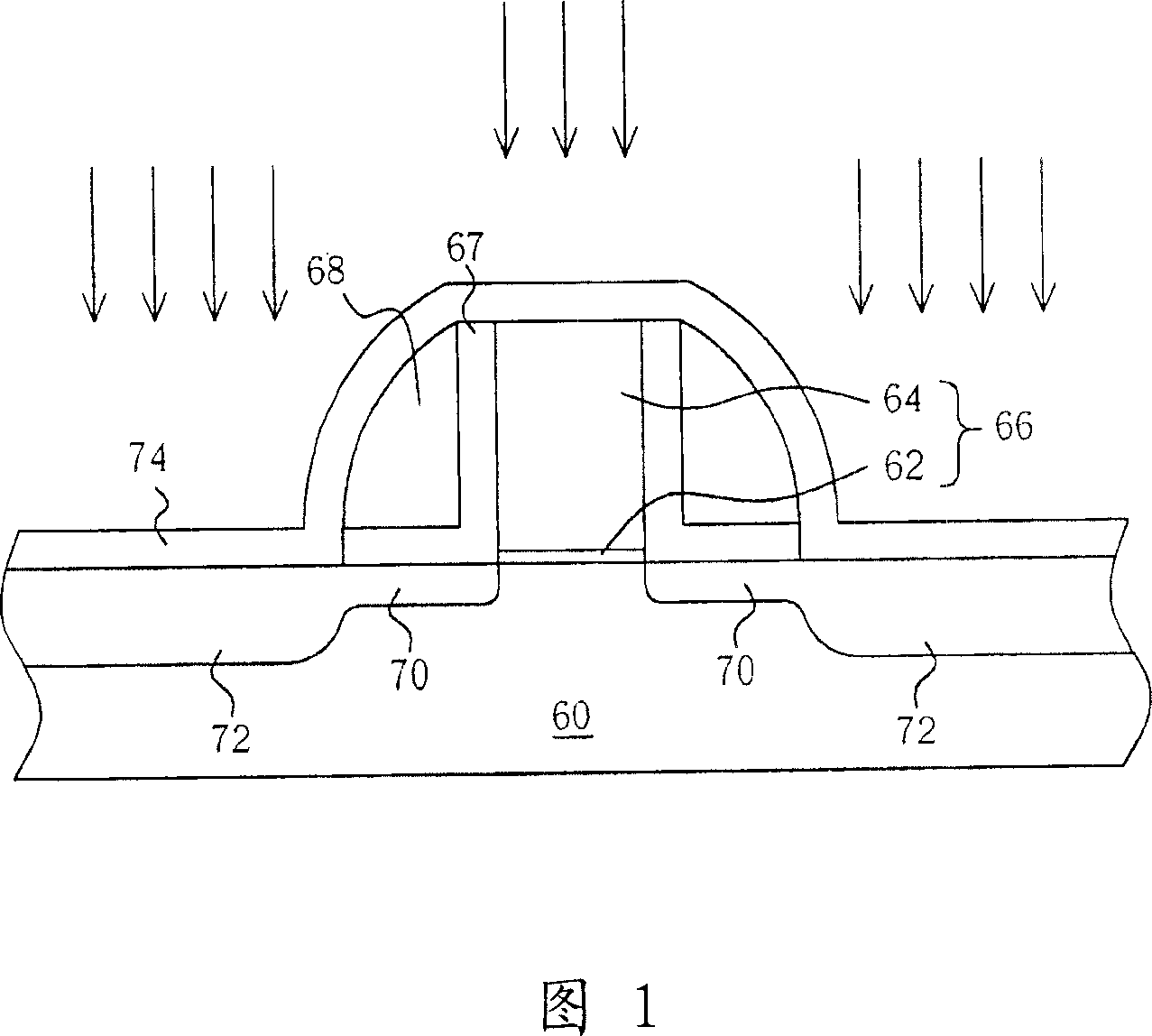
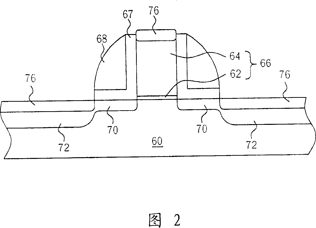
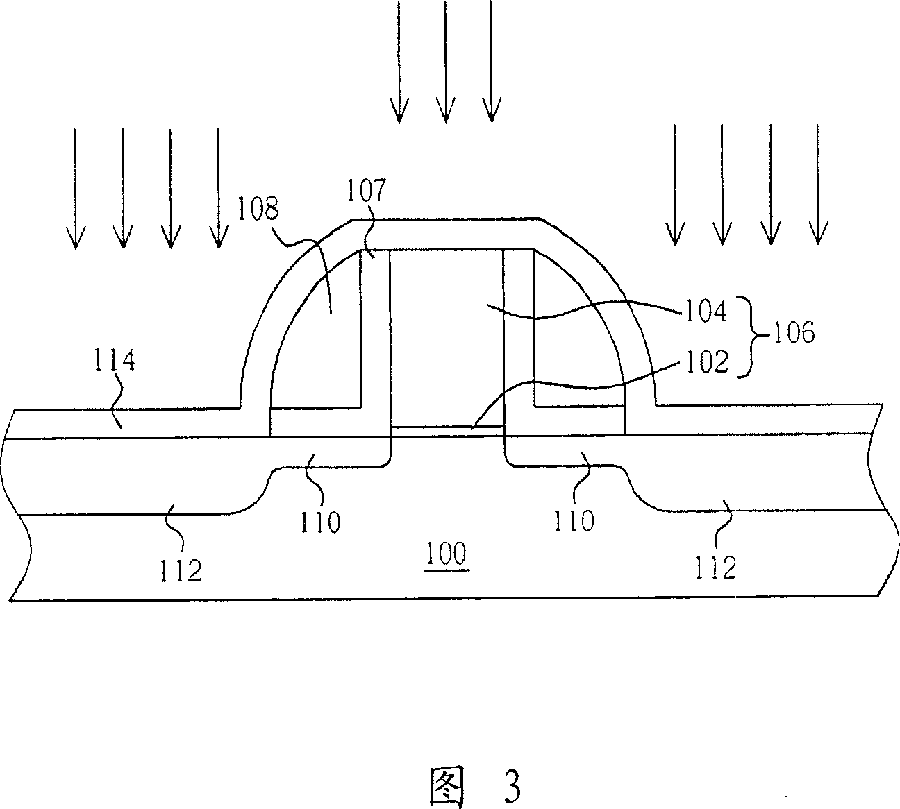
[0029] Please refer to FIG. 3 to FIG. 5. FIG. 3 to FIG. 5 are process schematic diagrams of applying the salicide process of the present invention to MOS transistors. As shown in FIG. 3, first, a substrate 100, such as a wafer or SOI substrate, is provided, and the surface of the substrate 100 has at least one silicon composed of monocrystalline silicon, polycrystalline silicon or epitaxial silicon. Conductive layer (not shown). Wherein, the silicon conductive layer can include gate, source / drain regions, word lines or resistors for different product requirements and process designs. In the preferred embodiment of the present invention, MOS The gate structure 102 and source / drain regions 112 of the transistor are described. As shown in FIG. 3, the gate structure 102 includes a gate dielectric layer 102 and a gate 104. The gate dielectric layer 102 is made of a dielectric material such as silicon dioxide, and the gate 104 is doped It is made of conductive materials such as doped po...


PUM


Abstract

The technique of self-aligned metal silicides (salicide) includes following steps: first providing a surface of containing at least a substrate of a silicon conductive layer; next, carrying out a degas step for the said substrate, and a cooling step for the substrate; then, depositing a metal layer on surface of the substrate, and the metal layer is contacted to the surface of the silicon conductive layer; carrying out a heat treatment in order to form a silicate metal layer on surface of the silicon conductive layer of contacting with the metal layer; finally, removing unreacted the metal layer.

Description

Technical field [0001] The present invention relates to a semiconductor device process, and in particular to a method for manufacturing salicide. Background technique [0002] In the process of semiconductor integrated circuits, metal-oxide-semiconductor (MOS) transistors are an extremely important electronic component. As the size of semiconductor components becomes smaller and smaller, there are many process steps for MOS transistors. The improvement to manufacture small and high-quality MOS transistors. [0003] The existing MOS transistor process involves forming a gate structure on a semiconductor substrate, and then forming a lightly doped drain (LDD) structure in the substrate on opposite sides of the gate structure. Next, spacers are formed on the sides of the gate structure, and the gate structure and the sidewalls are used as a mask to perform an ion implantation step to form source / drain regions in the semiconductor substrate. In order to properly electrically connect ...

Claims


Application Information

Patent Timeline
Patent Type & Authority Applications(China)
IPC IPC(8): H01L21/283H01L21/3205H01L21/768H01L21/336
Inventor 张毓蓝谢朝景江怡颖陈意维洪宗佑李佳蓉
Owner UNITED MICROELECTRONICS CORP
Why Eureka
Try Eureka