Method for forming secondary partition sheet used for strain silicon MOS transistor and structure thereof

一种隔片、栅极结构的技术,应用在晶体管、电固体器件、半导体器件等方向,能够解决困难、难制造、复杂制造工艺和结构等问题,达到增大空穴迁移率、改进工艺集成、高器件产率的效果

Active Publication Date: 2007-03-28
SEMICON MFG INT (SHANGHAI) CORP +1
View PDF0 Cites 4 Cited by
  • Summary
  • Abstract
  • Description
  • Claims
  • Application Information

AI Technical Summary

Problems solved by technology

Although significant improvements have been made, the design of such devices still has many limitations
Just as an example, these designs must get smaller and smaller, but still provide a clean signal for switching, which becomes more difficult as the device gets smaller
In addition, these designs are often difficult to manufacture and often require complex manufacturing processes and structures

Method used


Image

  • Method for forming secondary partition sheet used for strain silicon MOS transistor and structure thereof
  • Method for forming secondary partition sheet used for strain silicon MOS transistor and structure thereof
  • Method for forming secondary partition sheet used for strain silicon MOS transistor and structure thereof

Examples


Embodiment Construction

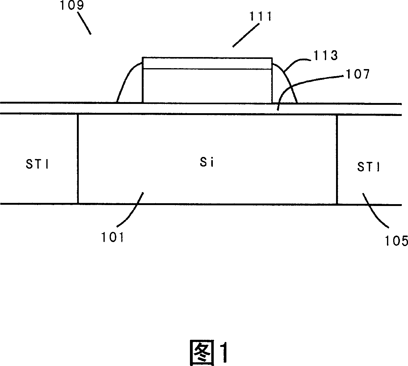
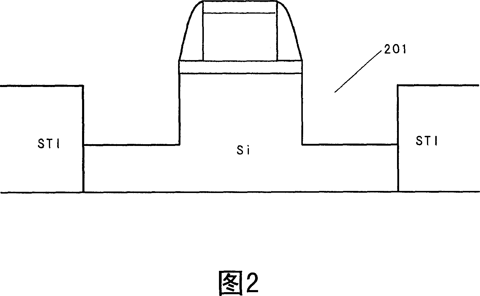
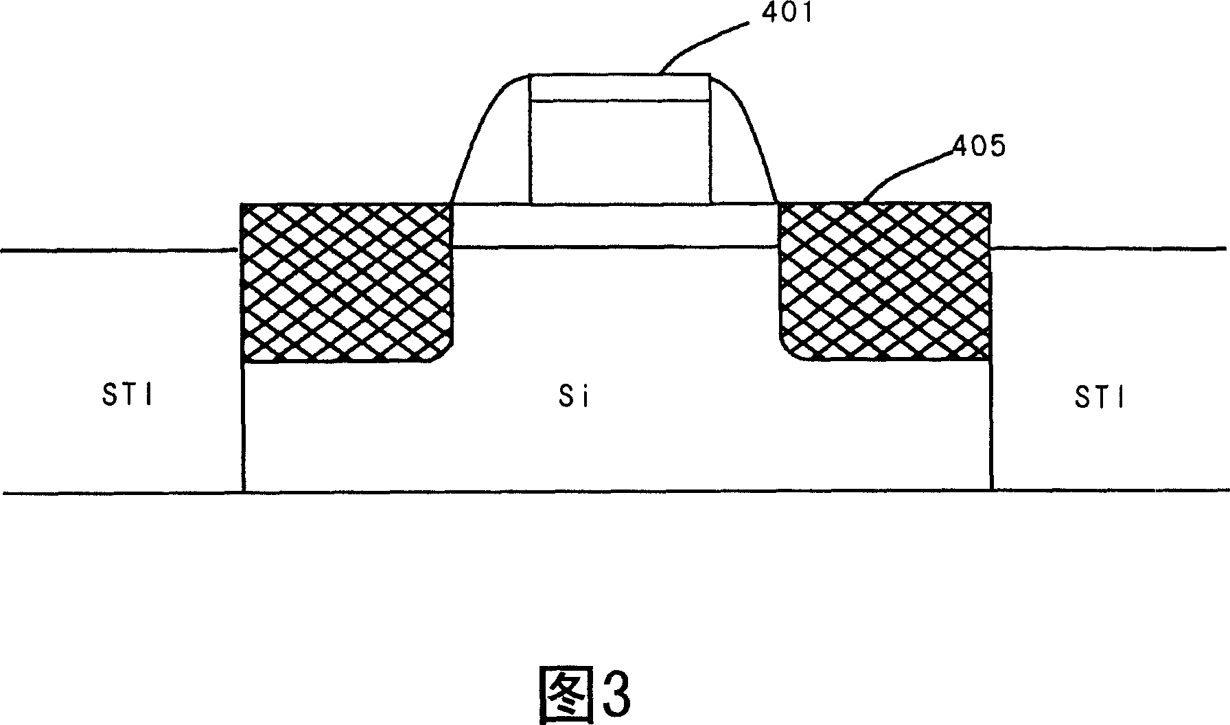
[0014] According to the present invention, there is provided a technique for processing integrated circuits for semiconductor device fabrication. More specifically, the present invention provides methods and structures for fabricating MOS devices using strained silicon structures for CMOS advanced integrated circuit devices. However, it should be realized that the present invention has broader applicability.

[0015] A method for manufacturing a CMOS integrated circuit device according to one embodiment of the present invention can be summarized as follows:

[0016] 1. Provide semiconductor substrates such as silicon wafers, silicon-on-insulator;

[0017] 2. Forming a dielectric layer (eg, gate oxide or nitride) overlying the semiconductor substrate;

[0018] 3. Forming a gate layer (eg, polysilicon, metal) overlying the dielectric layer;

[0019] 4. patterning the gate layer to form a gate structure comprising a plurality of edges (eg, a plurality of sides or edges);

[0...


PUM


Abstract

The method for forming CMOS supplies semiconductor substrate (ex. silicon wafer), and dielectric layer (ex. silica, silicon oxynitride) on the substrate. The method includes steps: forming grid layer of covering the dielectric layer, patternizing grid layer in order to form grid structure with multiple edges; forming dielectric layer on the grid structure in order to protect grid structure with multiple edges, and in optimization, thickness of the dielectric layer is smaller than 40 Nano; using the dielectric layer as protective layer to etch source region and drain region adjacent to the grid region to deposit materials of silicon, and germanium; materials of silicon, and germanium in source region and drain region make channel region between source region and drain region occur strain in compress mode. The method forms second protection layer of covering surface, and carries out anisotropic etching process in order to form struction of parting slip to seal grid structure.

Description

technical field [0001] The present invention relates to integrated circuits and their processing for the manufacture of semiconductor devices. More specifically, the present invention provides methods and structures for fabricating MOS devices using strained silicon structures for advanced CMOS integrated circuit devices. However, it should be realized that the present invention has broader applicability. Background technique [0002] Integrated circuits have grown from a handful of interconnected devices fabricated on a single silicon chip to millions of devices. Traditional integrated circuits offer performance and complexity far beyond what was originally imagined. To achieve increases in complexity and circuit density (i.e., the number of devices that can fit on a given chip area), with each generation of integrated circuits, the size of the smallest device linewidth (also referred to as device "geometry") becomes getting smaller and smaller. [0003] Increasing circ...

Claims


Application Information

Patent Timeline
Patent Type & Authority Applications(China)
IPC IPC(8): H01L21/336H01L21/8232H01L21/8238H01L29/78H01L27/04H01L27/092
CPCH01L29/66545H01L21/823807H01L21/823814H01L29/7848H01L29/66636H01L21/823864
Inventor 陈军宁先捷吴汉明
Owner SEMICON MFG INT (SHANGHAI) CORP
Why Eureka
Try Eureka