Semiconductor device and integrated circuit device

A semiconductor and conductive coating technology, applied in the manufacture of semiconductor devices, circuits, semiconductor/solid-state devices, etc., can solve the problems of limited use of porous dielectric layer materials, weak mechanical hardness, etc., to improve mechanical hardness and reduce signal delayed effect

Inactive Publication Date: 2007-04-18
TAIWAN SEMICON MFG CO LTD
View PDF0 Cites 3 Cited by
  • Summary
  • Abstract
  • Description
  • Claims
  • Application Information

AI Technical Summary

Problems solved by technology

[0006] The disadvantage of inherently weak mechanical hardness limits the use of porous dielectric layer materials

Method used


Image

  • Semiconductor device and integrated circuit device
  • Semiconductor device and integrated circuit device
  • Semiconductor device and integrated circuit device

Examples


Embodiment Construction

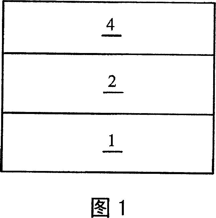
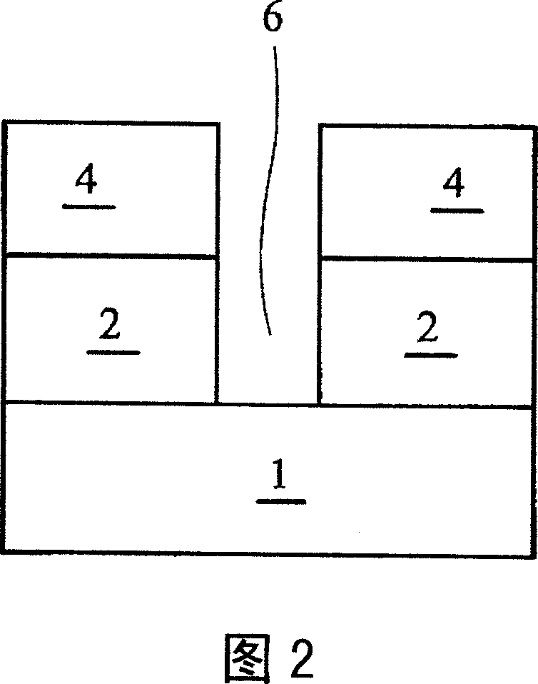
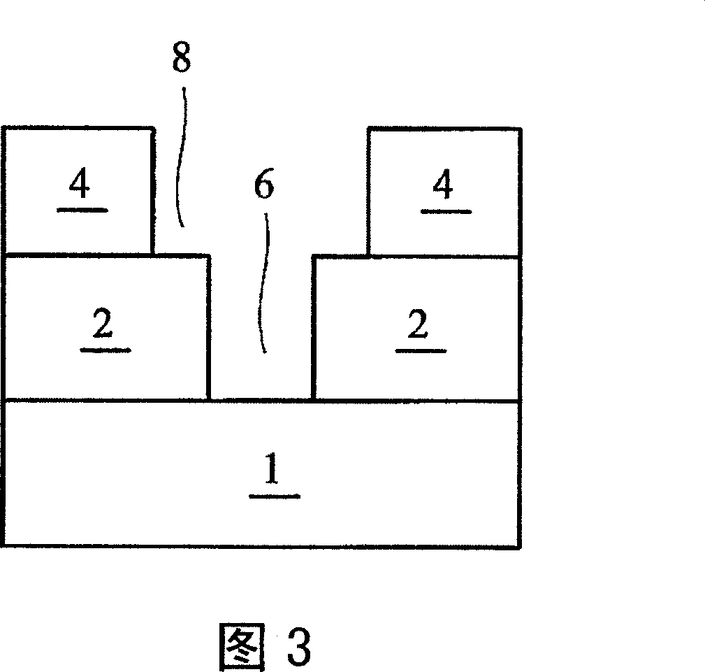
[0034] The preferred embodiment of the present invention integrates ultra-low-k dielectric layers and higher-k dielectric layers in a dual damascene process. FIGS. 1 to 7 and FIGS. 10 to 14 show cross-sectional views of intermediate stages of the process of preferred embodiments. In each embodiment of the present invention, the same symbols represent the same components.

[0035] Please refer to FIG. 1 , which shows the formation of a semiconductor device. Starting from the substrate 1 , a dielectric layer 2 , also referred to as a first dielectric layer 2 , is formed on the substrate 1 . The dielectric constant of the first dielectric layer 2 is preferably less than about 2.7, and the average porosity is greater than about 10%. There are many materials that can be used for the first dielectric layer 2, including but not limited to carbon-doped silicon oxides, fluorine-doped silicon oxides, organic low dielectric constant materials, and porous low dielectric constant material...


PUM


Abstract

A semiconductor structure includes a first dielectric layer having a k value of less than about 2.7, a second dielectric layer over the first dielectric layer, a via in the first dielectric layer, a conductive line in the second dielectric layer, wherein the conductive line extends from a top surface of the second dielectric layer into the second dielectric layer and electrically coupled to the via, a third dielectric layer on the second dielectric layer, and a fourth dielectric layer between the second dielectric layer and the conductive line. The second dielectric layer is preferably a porous material and has an ultra low k value. The k value of the second dielectric layer is lower than the k values of the first, the third and the fourth dielectric layers.

Description

technical field [0001] The present invention relates to the manufacturing process of semiconductor integrated circuits, in particular to the damascene process utilizing the dielectric layer of ultra-low dielectric constant. Background technique [0002] Integrated circuit technology has opened a new era in the semiconductor industry due to the advantages of reducing the size of components to increase the density of components. Component density is limited by the capabilities of the lithography process, and shrinking component dimensions creates new constraints. For example, for any two adjacent conductors, the closer the distance between the conductors is, the larger the capacitance (which is a function of the distance between the two conductors and the dielectric constant (k) of the material of the insulating layer therebetween) is greater. An increase in capacitance results in increased capacitive coupling and power dissipation between the two conductors, thus slowing dow...

Claims


Application Information

Patent Timeline
Patent Type & Authority Applications(China)
IPC IPC(8): H01L23/532
CPCH01L21/76814H01L21/76807H01L21/76829H01L21/76835H01L21/76831H01L21/76826
Inventor 鲁定中陈学忠
Owner TAIWAN SEMICON MFG CO LTD
Why Eureka
Try Eureka