High pressure metal oxide semiconductor element and its manufacturing method
A technology of oxide semiconductor and manufacturing method, applied in semiconductor/solid-state device manufacturing, semiconductor devices, electrical components, etc., can solve problems such as limited capacity, and achieve the effect of improving breakdown voltage
- Summary
- Abstract
- Description
- Claims
- Application Information
AI Technical Summary
Problems solved by technology
Method used
Image

Examples
Embodiment Construction
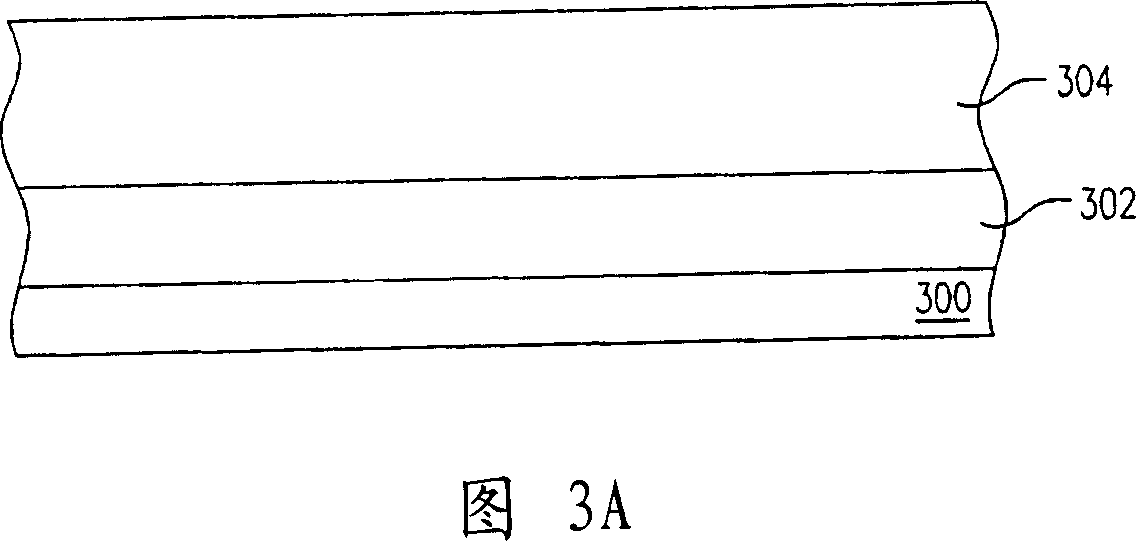
[0055] 3A to 3D are cross-sectional views showing the manufacturing process of the metal-oxide-semiconductor transistor device according to an embodiment of the present invention.
[0056] Referring to FIG. 3A , firstly, a substrate 300 is provided. The substrate 300 is, for example, an N-type silicon substrate.
[0057] Next, a buried N-type doped region 302 is formed in the substrate 300 . The buried N-type doped region 302 is formed by, for example, performing an ion implantation process using phosphorus as a dopant.
[0058] Then, an N-type epitaxial layer 304 is formed on the substrate. The method for forming the N-type epitaxial layer 304 is, for example, using phosphorus as a dopant to perform a chemical vapor deposition process in an in-situ doping method to form a layer of amorphous silicon material (not shown), and then the amorphous silicon material layer formed by a solid phase epitaxy step.
[0059] Next, please refer to FIG. 3B , an N-type well region 306 is ...
PUM
 Abstract
Description
Claims
Application Information