Novel semiconductor material In-Ga-N surface barrier type solar battery and its preparation method

A surface barrier, solar cell technology, applied in semiconductor devices, circuits, photovoltaic power generation, etc., can solve the problems of solar cells that have not been reported in domestic and foreign literature, and achieve the effects of reducing interface recombination, high absorption coefficient, and light weight

Inactive Publication Date: 2007-05-30
NANJING UNIV
View PDF0 Cites 8 Cited by
  • Summary
  • Abstract
  • Description
  • Claims
  • Application Information

AI Technical Summary

Problems solved by technology

[0005] At present, any type of solar cell made of InGaN has not been reported in the literature at home and abroad.

Method used


Image

  • Novel semiconductor material In-Ga-N surface barrier type solar battery and its preparation method
  • Novel semiconductor material In-Ga-N surface barrier type solar battery and its preparation method

Examples


Embodiment Construction

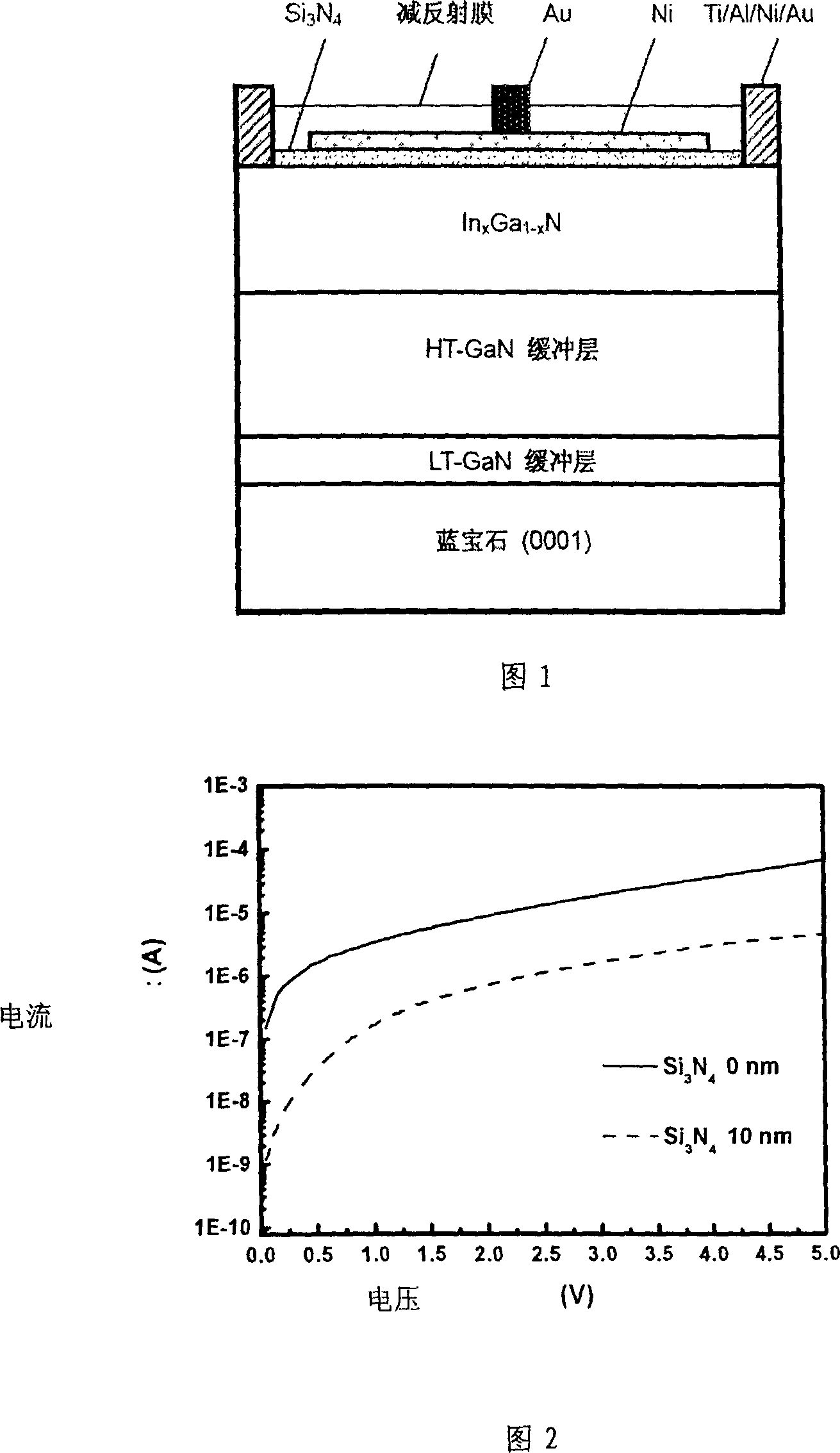
[0020] The structure of the InGaNMIS surface barrier solar cell shown in Figure 1 is grown sequentially on the c-plane (0001) sapphire substrate material: low temperature GaN (LT-GaN) buffer layer, high temperature GaN (HT- GaN) buffer layer, In x Ga 1-x N light absorbing layer, Si 3 N 4 insulating layer, and the Si 3 N 4 The insulating layer is provided with Schottky contact metal, in n-In x Ga 1-x Conductive electrodes are arranged on the N layer. The structure of the InGaN MS surface barrier solar cell is the same as above, except that Si is not grown 3 N 4 insulating layer, directly on the In x Ga 1-x A Schottky contact metal is provided on the surface of the N layer.

[0021] The material growth method is: using MOCVD method to use (0001) sapphire as the substrate to first grow a low-temperature GaN buffer layer, the growth temperature is in the range of 500-700°C, and the thickness is in the range of 20-200nm, and then the low-temperature GaN buffer layer is 9...


PUM

PropertyMeasurementUnit
thicknessaaaaaaaaaa
thicknessaaaaaaaaaa
thicknessaaaaaaaaaa

Abstract

This invention relates to Incan surface barrier solar batter, which is processed by the following steps: selecting semiconductor materials InxGa1-xN(0<=x<=1) as light absorptive area and InxGa1-xN MS or MIS structures; growing GaN buffer layer with thickness of 20 to 200 nm on aquamarine underlay and then after annealing growing high temperature GaN buffer layer with 1000 to 2000nm and InxGa1-XN layer; then forming Scotty structure by setting Scotty probe metal Ni and thick lead wire on InxGa1-xN; depositing Si3N4 insulation film on InxGal-xN and then setting Scotty probe metal and lead metal to form the structure.<0}.

Description

technical field [0001] The invention relates to a semiconductor solar cell. In particular, a new semiconductor material for solar cells, In x Ga 1-x N and In x Ga 1-x A method for preparing an N surface barrier type solar cell. Background technique [0002] Since the 1990s, research on the application of Group III nitride materials and devices such as semiconductor gallium nitride GaN and its alloys such as aluminum gallium nitride AlGaN and indium gallium nitride InGaN has developed rapidly, mainly used in optoelectronic devices and high-frequency high-power microelectronic devices. In 2002, W.Walukiewicz and others in the United States found that the band gap of InN was 0.7eV, see J.Wu, W.Walukiewicz, K.M.Yu, J.W.Ager III, E.E.Haller, H.Lu, W.J.Schaff, Y.Saito, and Y. Nanishi, Appl. Phys. Lett. 80, 3967 (2002), instead of 1.89 eV as previously reported. This makes In x Ga 1-x The band gap of N alloy is continuously adjustable from 3.4eV of GaN (X=0) to 0.7eV of InN...

Claims


Application Information

Patent Timeline
Patent Type & Authority Applications(China)
IPC IPC(8): H01L31/078H01L31/18
CPCY02E10/50Y02P70/50
Inventor 江若琏谢自力张荣文博周建军刘斌陈敦军郑有炓韩平刘成祥
Owner NANJING UNIV
Why Eureka
Try Eureka