Method of manufacturing structure

a manufacturing method and structure technology, applied in the field of manufacturing structures, can solve problems such as setting the conditions for applying structures, and achieve the effect of satisfying anti-reflection performance and great effect on the quality of optical elements

Inactive Publication Date: 2018-07-17
FUJIFILM CORP
View PDF18 Cites 2 Cited by
  • Summary
  • Abstract
  • Description
  • Claims
  • Application Information

AI Technical Summary

Benefits of technology

[0006]The boehmite fine uneven structure has satisfactory antireflection performance. However, in a case of forming a structure by the method of the related art as described in JP2005-275372A, scattered light is generated at a low but intolerable level. The scattered light is recognized as fogging on the coated surface of an optical element and has a great effect on the quality of the optical element. The present inventors thought that the reason for causing the fogging in the optical element is that a boehmite fine uneven structure is random. That is, it is thought that in a case in which a large number of fluctuation components having a large size of about the wavelength of light or larger are present in the boehmite fine uneven structure, the fine uneven structure has an effect on light scattering. In this manner, in the optical element including the fine uneven structure as an antireflection structural body or the like, a finer uneven structure in which a long-period fluctuation is reduced is demanded.
[0010]The present invention is made in consideration of the above circumstances and an object thereof is to provide a method of manufacturing a structure including a transparent fine uneven structural body which is obtained by hot water treatment without requiring an accurate liquid phase process, in which scattered light can be reduced and a finer uneven structure can be formed.
[0014]Based on the above idea, in a case in which the peak value of the space frequency of a fine uneven structure that is intentionally formed before hot water treatment is greater than the peak value of the space frequency in a case of performing hot water treatment without forming a fine uneven structure, the peak value of the space frequency of the fine uneven structure formed by forming the fine uneven structure before hot water treatment and then performing the hot water treatment is positioned to be closer to a high-frequency side. Scattered light is generated in a case in which particularly, a component of equal to or greater than the wavelength order (wavelength / refractive index of medium) is present in the spatial range. Therefore, light scattering is reduced by setting the space frequency distribution to be on a high-frequency side.
[0024]The fine uneven structure formed in the second step is not limited to a fine uneven structure which is periodically formed and any arrangement can be employed as long as the uneven structure satisfies Expression I in the precursor film. In addition, in order to obtain the maximum effect, it is desirable that this uneven structure is formed over the entire optically effective surface. However, in a case in which least a part of the uneven structure satisfying Expression I is present in the optically effective surface, it is possible to obtain the effect on the region. Therefore, as the ratio of the uneven structure formed region occupying the optically effective surface increases, the effect is more likely to be obtained. Thus, it is desirable that the region becomes larger.

Problems solved by technology

However, in the preparation step of the uneven structure disclosed in JP2014-081656A, an accurate liquid phase process in which a single particle film has to be prepared on the surface of a sample or the like before the uneven structure is formed is required, and thus there is a problem of difficulty in setting conditions for applying the structure to optical elements having various shapes such as a concave surface and a convex surface.

Method used


Image

  • Method of manufacturing structure
  • Method of manufacturing structure
  • Method of manufacturing structure

Examples


example 1

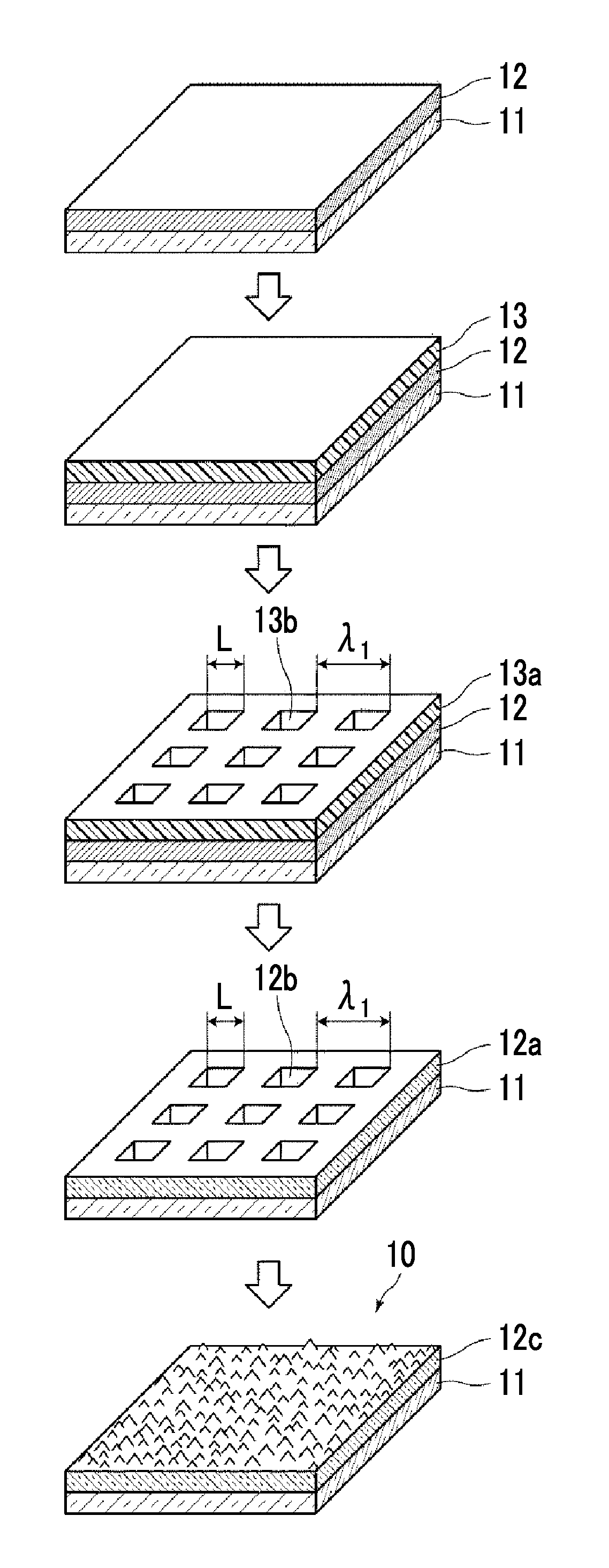
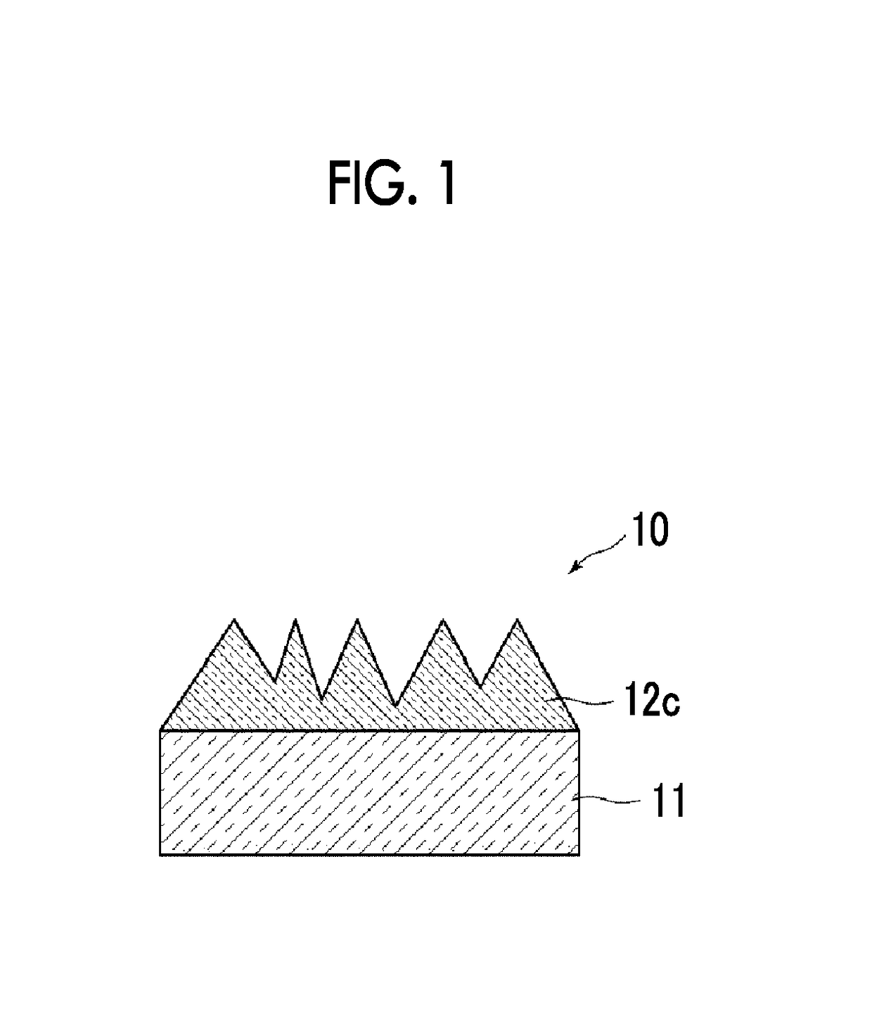
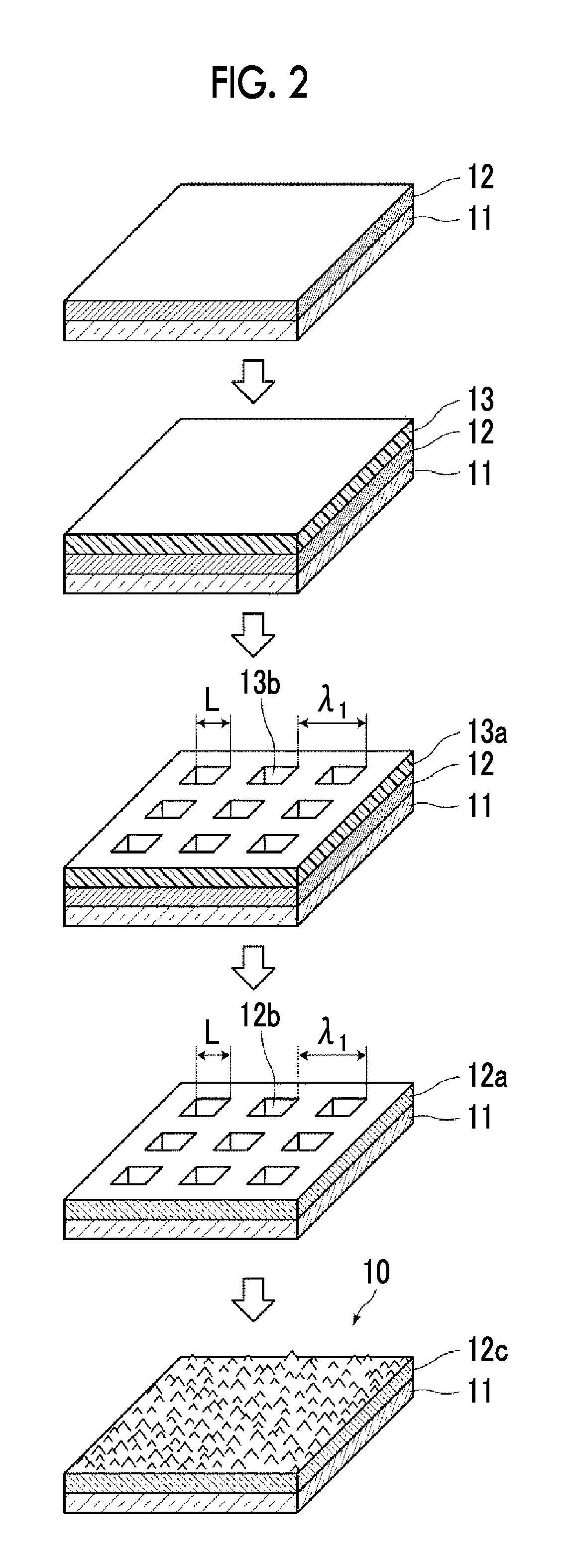
[0107]Hereinafter, the manufacturing method in a case in which the structure of the present invention is an optical member will be described.

[0108](First Step)

[0109]First, synthetic quartz glass (product name “AQ”, manufactured by Asahi Glass Co., Ltd.) which is a transparent substrate was used as the substrate. On the transparent substrate, a thin alumina (Al2O3) film was formed as the precursor film by electron cyclotron resonance sputtering (ECR) (device name “AFTEX-6000”, manufactured by JSW AFTY Corporation) to have a thickness of 80 nm.

[0110](Second Step)

[0111]Next, a resist film for electron beams (product name “FEP-171”, manufactured by Fujifilm Electronic Materials Co., Ltd.) was applied onto the thin alumina film.

[0112]On the entire surface of the resist film for electron beams, a periodic pattern having square openings in which a length of one side is 100 nm arranged at an interval of 200 nm period was drawn by an electronic beam. Then, the resist film was developed to ob...

example 2

[0121]Example 2 shows a manufacturing method in a case in which the structure is an optical member and a fine uneven structure is formed by using an Ag-deposited mask.

[0122](First Step)

[0123]First, synthetic quartz glass (product name “AQ”, manufactured by Asahi Glass Co., Ltd.) which is a transparent substrate was used as the substrate. On the transparent substrate, a thin alumina (Al2O3) film was formed as the precursor film by electron cyclotron resonance sputtering (ECR) (device name “AFTEX-6000”, manufactured by JSW AFTY Corporation) to have a thickness of 80 nm.

[0124](Second Step)

[0125]Next, Ag was deposited onto the thin alumina film by electron beam (EB) deposition (device name “EVD-1501”, manufactured by CANON ANELVA CORPORATION) so as to have a target film thickness of 5 nm. Through self-organization of Ag, Ag particles having a diameter of about 20 to 60 nm were formed over the entire surface of the thin alumina film in a state in which a large number of particles were fo...

example 3

[0130]Example 3 shows a manufacturing method in a case in which the structure is an optical member and a fine uneven structure is subjected to plasma etching without using a mask.

[0131](First Step)

[0132]First, synthetic quartz glass (product name “AQ”, manufactured by Asahi Glass Co., Ltd.) which is a transparent substrate was used as the substrate. On the transparent substrate, a thin alumina (Al2O3) film was formed as the precursor film by electron cyclotron resonance sputtering (ECR) (device name “AFTEX-6000”, manufactured by JSW AFTY Corporation) to have a thickness of 80 nm.

[0133](Second Step)

[0134]Subsequently, the thin alumina film was subjected to plasma etching (device name “NE-500”, manufactured by CANON ANELVA CORPORATION) for 50 seconds. For the etching conditions, the process pressure was set to 1.0 Pa, the etching gas was set to CHF3 / Ar=5 / 25, and the radio frequency (RF) output (Ant / Bias) was set to 700 / 50 W. The thin alumina film was etched to a depth film thickness o...


PUM

PropertyMeasurementUnit
acceleration voltageaaaaaaaaaa
wavelength rangeaaaaaaaaaa

Abstract

Provided is a method of manufacturing a structure having a transparent fine uneven structural body formed by hot water treatment, in which a finer uneven structure is formed. Provided is a method of manufacturing a structure, the method being for manufacturing a structure including a substrate, and a transparent fine uneven structural body which is formed on a surface of the substrate by hot water treatment, including: a first step of forming a precursor film of the transparent fine uneven structural body on the substrate; a second step of forming a fine uneven structure on a surface of the precursor film; and a third step of subjecting, to hot water treatment, the precursor film on which the fine uneven structure is formed to form the transparent fine uneven structural body in which a peak value ν0 of space frequency of the unevenness of the fine uneven structure formed in the second step satisfies ν<ν0 (Expression I). In Expression I, ν0 represents a peak value of space frequency of the fine uneven structure, and ν represents a peak value of space frequency of the transparent fine uneven structural body in a case in which the fine uneven structure is not formed on the surface of the precursor film.

Description

CROSS-REFERENCE TO RELATED APPLICATIONS[0001]This application is a continuation application of International Application No. PCT / JP2016 / 001556, filed Mar. 17, 2016, the disclosure of which is incorporated herein by reference in its entirety. Further, this application claims priority from Japanese Patent Application No. 2015-085648, filed Apr. 20, 2015, the disclosure of which is incorporated herein by reference in its entirety.BACKGROUND OF THE INVENTION1. Field of the Invention[0002]The present invention relates to a method of manufacturing a structure including a transparent fine uneven structural body which is obtained by hot water treatment.2. Description of the Related Art[0003]In the related art, in a lens (transparent substrate) formed by using a light-transmitting member such as glass or a plastic, an antireflection structural body is provided on a light incident surface in order to reduce the loss of transmitted light caused by surface reflection. As an antireflection struc...

Claims


Application Information

Patent Timeline
Patent Type & Authority Patents(United States)
IPC IPC(8): G02B1/118C03C17/25
CPCG02B1/118C03C17/25C03C2217/214B32B3/30C03C17/245C03C2217/28C03C2217/732C03C2218/32C03C2218/33C03C2218/34G02B1/12
Inventor YOSHIZAWA, HIROTOSHISONODA, SHINICHIROYOSHIHIRO, TATSUYA
Owner FUJIFILM CORP
Why Eureka
Try Eureka