Conductive substrate and method for manufacturing same

a technology of conducting substrate and manufacturing method, which is applied in the direction of conductors, sustainable manufacturing/processing, and final product manufacturing, etc., can solve the problems of increasing the price of the substrate, the method is not a reasonable method, etc., and achieves the effect of reducing resistance loss, simple process and efficient conducting substra

Active Publication Date: 2018-08-14
LG DISPLAY CO LTD
View PDF22 Cites 1 Cited by
  • Summary
  • Abstract
  • Description
  • Claims
  • Application Information

AI Technical Summary

Benefits of technology

[0019]According to exemplary embodiments of the present invention, an efficient conducting substrate can be formed by a simple process. Further, in the present invention, an amorphous transparent conducting layer and a metal layer are introduced to minimize resistance loss of a crystalline transparent conducting layer.
[0020]Further, according to exemplary embodiments of the present invention, since the conducting substrate can be prepared without introducing an additional insulating layer formed on a secondary substrate in the related art, the number of processes can be reduced, and as a result, the competitive price can be secured.

Problems solved by technology

However, this method is not a reasonable method because the number of processes is many and an increase in price of a substrate occurs.

Method used


Image

  • Conductive substrate and method for manufacturing same
  • Conductive substrate and method for manufacturing same
  • Conductive substrate and method for manufacturing same

Examples


example 1

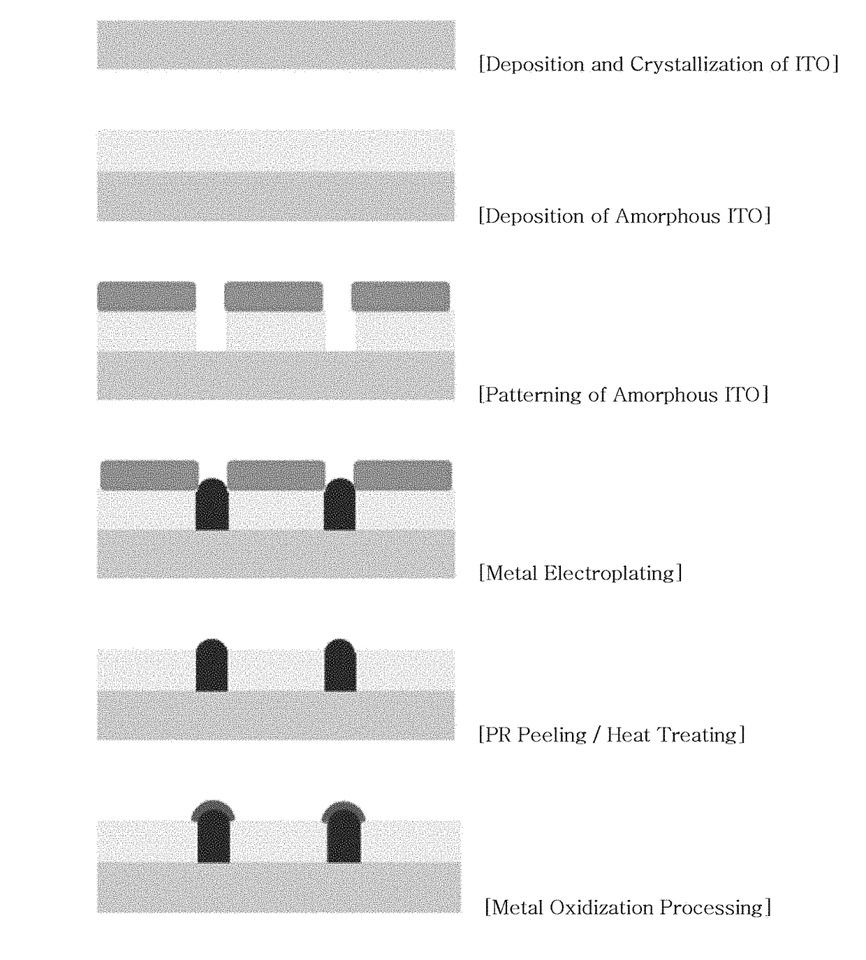
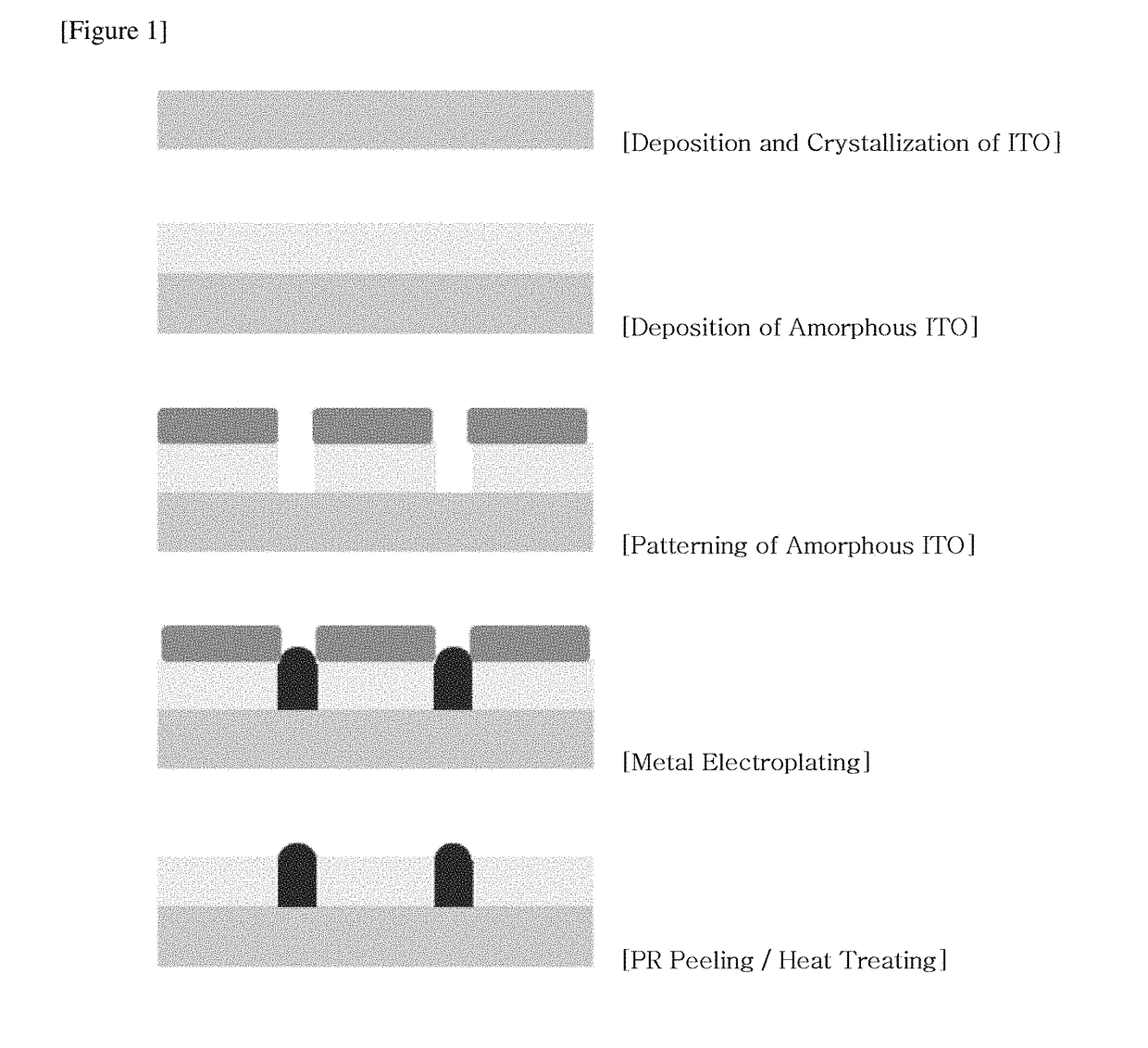
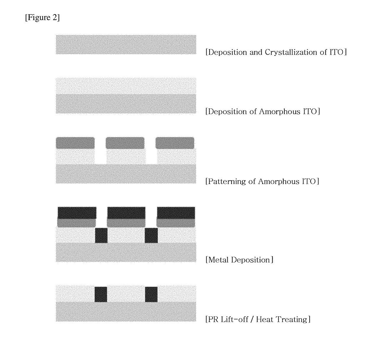
1) Forming Crystalline Transparent Conducting Layer on Glass Substrate

[0086]A crystalline indium tin oxide (ITO) thin film having a thickness of 300 nm was formed on a glass substrate by using materials and conditions described below. Specific resistance of the prepared crystalline ITO thin film was 2×10⁻⁴ Ωcm.

[0087]Deposition temperature: 400° C. (using RF Magnetron sputter)

[0088]Target: In2O3:SnO2=90 mol %:10 mol % purity 99.99% (Cerac Co)

[0089]RF Power: 150 W

[0090]Deposition Conditions: deposition time (30 min), pressure (10 mtorr)

[0091]Post heat treatment: 400° C. for 1 min

2) Forming Amorphous Transparent Conducting Layer on Crystalline Transparent Conducting Layer

[0092]An amorphous ITO thin film having a thickness of 300 nm was formed on a crystalline ITO thin film by using materials, equipment, and conditions below. Specific resistance of the prepared amorphous ITO thin film was 10×10−4 Ωcm.

[0093]Deposition temperature: 110° C. (using RF Magnetron sputter)

[0094]Target: In2O3:S...

example 2

[0100]After the metal electroplating according to Example 1 above, a metal oxide layer was formed by heat treatment at 500° C. for approximately 30 min under an oxygen atmosphere by using RTA equipment through electroless plating.

[0101]According to exemplary embodiments of the present invention, an efficient conducting substrate can be formed by a simple process. Further, in the present invention, an amorphous transparent conducting layer and a metal layer are introduced to minimize resistance loss of a crystalline transparent conducting layer.

[0102]Further, according to exemplary embodiments of the present invention, since the conducting substrate can be prepared without introducing an additional insulating layer formed on a secondary substrate in the related art, the number of processes can be reduced, and as a result, the competitive price can be secured.


PUM

PropertyMeasurementUnit
glass transition temperatureaaaaaaaaaa
Tgaaaaaaaaaa
transparentaaaaaaaaaa

Abstract

An exemplary embodiment of the present invention comprises: 1) forming a crystalline transparent conducting layer on a substrate; 2) forming an amorphous transparent conducting layer on the crystalline transparent conducting layer; 3) forming at least one pattern open region so as to expose a part of the crystalline transparent conducting layer by patterning the amorphous transparent conducting layer; and 4) forming a metal layer in the at least one pattern open region.

Description

[0001]This application is a National Phase entry of PCT / KR2013 / 011072 filed on Dec. 2, 2013 and claims priority to Korean Application Nos. 10-2012-0138364 and 10-2012-0138340 both filed Nov. 30, 2012, all of which are incorporated by reference for all purposes as if fully set forth herein.TECHNICAL FIELD[0002]This application claims priority from Korean Patent Application Nos. 10-2012-0138364 and 10-2012-0138340 filed on Nov. 30, 2012 in the KIPO, the disclosure of which is incorporated herein by reference in its entirety.[0003]The present invention relates to a conducting substrate and a method for preparing the same.BACKGROUND ART[0004]In the related art, a cathode electrode of an organic light emitting device, an organic solar cell, or the like basically uses indium tin oxide (ITO) as a primary electrode and primarily uses a secondary electrode made of metal in order to prevent loss of optical efficiency by high resistance of the ITO, and the like.[0005]In a method for forming th...

Claims


Application Information

Patent Timeline
Patent Type & Authority Patents(United States)
IPC IPC(8): H05K1/09H05K1/02H05K3/46H01L51/00H01B1/02H05K3/06C25D5/02H01L51/44H01L51/52
CPCH05K1/09H01B1/023H01L51/0023H01L51/445H05K1/0298H05K3/06H05K3/46C25D5/02Y02P70/521H01L51/442H01L51/5215H01L51/5234H01L2251/305H01L2251/308H05K2201/0326H05K2201/0329Y02E10/549H10K30/83Y02P70/50H10K71/621H10K30/82H10K50/816H10K50/828H10K2102/101H10K2102/103H01B13/00H10K99/00
Inventor HWANG, JI YOUNGSEONG, JIEHYUNSON, YONG GOO
Owner LG DISPLAY CO LTD
Why Eureka
Try Eureka