Method of manufacturing printed circuit board

a manufacturing method and printed circuit board technology, applied in the direction of printed element electric connection formation, circuit masks, printed circuit non-printed electric components, etc., can solve the problems of not being able to make direct electrical contacts such as flip-chip bonding between the chip electrode and the pads on the package substrate, and not being able to directly mount the semiconductor chip b>, etc., to achieve the effect of reducing manufacturing costs and enhancing integrating density

Active Publication Date: 2018-10-16
DAEDUCK ELECTRONICS
View PDF15 Cites 11 Cited by
  • Summary
  • Abstract
  • Description
  • Claims
  • Application Information

AI Technical Summary

Benefits of technology

[0015]This invention makes it possible to make direct electrical contacts of the semiconductor chip such as flip-chip bonding at the bottom surface of the cavity, which thereby enhances the integrating density as well as the reduction of the manufacturing cost.

Problems solved by technology

Since the bottom surface of the cavity tends to be inevitably non-flat when the laser drill is applied, it is not easy to directly mount the semiconductor chip 30 on the bottom surface of the cavity.
In other words, it is difficult to mount the semiconductor chip on the surface of the cavity due to the failure of surface flatness if the bottom surface of the cavity is severely damaged during the laser drill.
However, if you mount the semiconductor chip 30 on the copper barrier according to the prior art, you may succeed to embed the chip 30 just inside the cavity, but failed to make direct electrical contacts such as flip-chip bonding between the chip electrodes and the pads on the package substrate.
Recently, the number of I / O terminals has so tremendously increased that we will need a huge number, therefore a huge area for bonding pads if we adopt only the wire bonding technology, which will consequently increase the package size as well as the packaging cost.
Furthermore, as shown in FIG. 1c, if you want to realize a die stack, it is more difficult to make electrical contacts.
However, this method is not recommended because the bump pads are easily peeled off due to the non-uniformity of resin etching between the pads as well as non-uniformity in the resin depth of the bump.

Method used


Image

  • Method of manufacturing printed circuit board
  • Method of manufacturing printed circuit board
  • Method of manufacturing printed circuit board

Examples


Embodiment Construction

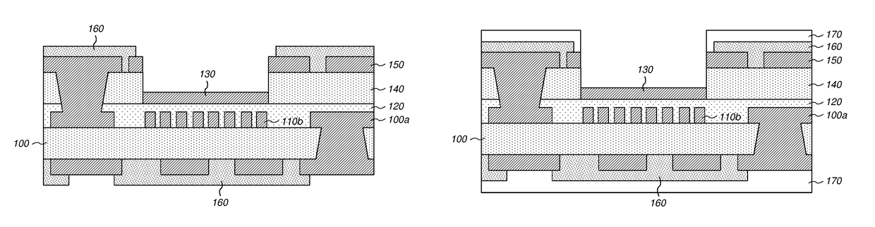
[0018]Detailed descriptions will be made on preferred embodiments and constitutional features of the fabricating method in accordance with the present invention with reference to attached figures from FIG. 2a to FIG. 2f.

[0019]The starting material in accordance with a preferred embodiment of the present invention is a structure comprising a first insulating layer such as resin or epoxy resin, of which the surface is coated with a copper layer. As a preferred embodiment of the present invention, a CCL (copper cladded laminate) or carrier copper can be utilized for coreless process.

[0020]FIG. 2a is a schematic diagram illustrating the intermediate step of manufacturing the package substrate in accordance with the present invention. Referring to FIG. 2a, a first copper layer with circuit pattern transferred is formed on the surface of the first insulating layer 100. By processing the image process comprising dry film coating, exposure, development, and etch, a general circuit 110a and...


PUM

PropertyMeasurementUnit
insulatingaaaaaaaaaa
surface flatnessaaaaaaaaaa
sizeaaaaaaaaaa

Abstract

A step of forming bump pads on the surface of the substrate corresponding to the cavity region, and covering the whole surface with a second insulating layer, forming a copper barrier on the surface of a second insulating layer corresponding to the cavity region for protection of the second insulating layer, forming a third insulating layer, and forming a copper layer for electrical circuit. A mask is formed on the copper later of the external circuit so that only the cavity region is exposed. The cavity is formed by laser-drilling only the surface-exposed area of the third insulating layer. The bottom copper layer protects the second insulating layer and bump pads underneath from laser damages. The copper barrier is removed by chemical etch after the laser drill. The second insulating layer with the bottom surface exposed will be removed via sand blast process, exposing the bump pads fabricated.

Description

CROSS REFERENCE TO RELATED APPLICATION[0001]This application claims priority under 35 USC § 119 to Korean Patent Application No. 10-2016-021772, filed on Feb. 24, 2016, the contents of which are incorporated herein by reference in their entirety. The list of the prior art is the following: Korean Patent Publication No. 10-2013-0096381, Korean Patent No. 139,273, Korean Patent No. 101,580,472.FIELD OF THE INVENTION[0002]The present invention relates to a method of manufacturing a Cavity for mounting and / or embedding a chip on the Printed Circuit Board (PCB) and more particularly a method of fabricating the bump pads on the bottom surface of the cavity which is the place not just for embedding and fixing the chip but for making electrical contacts like flip-chip contacts.BACKGROUND OF THE INVENTION[0003]Recently, a great deal of research and development (R&D) efforts are made on the semiconductor package. The conventional 2D (two-dimensional) package technology is now stepping forward...

Claims


Application Information

Patent Timeline
Patent Type & Authority Patents(United States)
IPC IPC(8): H01L23/00H05K3/46H05K3/40H05K3/42H05K3/10H05K3/00H05K1/18
CPCH01L24/03H05K3/0026H05K3/0035H05K3/0073H05K3/0079H05K3/10H05K3/40H05K3/4038H05K3/4061H05K3/429H05K3/4644H05K3/4679H05K3/4697Y10T29/49169Y10T29/49165Y10T29/4913H05K2203/107H05K2203/025H01L24/48H01L2224/0347H01L2224/16145H01L2224/48091H01L2224/48227H01L2224/73257H01L2924/00014H01L2924/181H05K1/182H05K2201/10674H01L2224/45099H01L2924/00012H01L21/4857H05K1/183H05K3/30H05K2201/09036H01L2924/15313H01L2924/15153H01L2224/73265H01L2224/32245H01L2224/73253H01L2224/16227H01L2224/16238H01L24/16H01L24/32H01L24/73
Inventor KO, YOUNG-JOOKO, TAE-HYUKLEE, HYEUNG-DO
Owner DAEDUCK ELECTRONICS
Why Eureka
Try Eureka