Integrated circuit heat dissipation using nanostructures

a technology of integrated circuits and nanostructures, applied in the direction of semiconductor devices, semiconductor/solid-state device details, electrical devices, etc., can solve the problems of reducing the performance and/or useful life of the device, limiting the operation of the device, and severely limited switch performance, etc., to achieve high thermal conductivity

Active Publication Date: 2018-10-23
IBM CORP
View PDF29 Cites 4 Cited by
  • Summary
  • Abstract
  • Description
  • Claims
  • Application Information

AI Technical Summary

Benefits of technology

[0006]In another aspect of the invention, a method of manufacturing a semiconductor structure includes forming an isolation layer on an electrically conductive feature of an integrated circuit device. The method includes forming an electrically conductive layer on the isolation layer. The method also includes forming a plurality of nanowire structures on a surface of the electrically conductive layer. The isolation layer is formed to electrically isolate the electrically conductive feature from the electrically conductive layer. The plurality of nanowire structures are formed of a high thermal conductivity material that provides a heat path away from the electrically conductive feature.
[0007]In yet another aspect of the invention, a semiconductor structure includes: an isolation layer on an electrically conductive feature of an integrated circuit device; an electrically conductive layer on the isolation layer; and a plurality of nanowire structures on a surface of the electrically conductive layer. The isolation layer electrically isolates the electrically conductive feature from the electrically conductive layer. The plurality of nanowire structures are composed of a high thermal conductivity material that provides a heat path away from the electrically conductive feature.

Problems solved by technology

Accumulation of heat within a device, such as a FET, can reduce the performance and / or useful lifetime of the device.
Heat generation is a limiting factor to improving device operation in many technologies.
For example, in radio frequency (RF) CMOS, switch performance is severely limited by the heat generated by the switch at high frequency.
This large amount of current flow over a relatively small region can result in heating of the devices up to 200° C. in the case of an RF amplifier.
These elevated temperatures can significantly change the characteristics of the devices, as well as degrade the integrity of its construction materials.
Further amplifying this problem is the desire to remove or reduce the number of electrical contacts in order to lower the capacitance of the devices, which will increase the need to dissipate heat because the electrical contacts do provide a path for the heat to escape.
Similar heat-related issues are present in the bipolar junction transistor (BJT) devices that are commonly used in radar and collision avoidance.
Passive structures, such as resistors, are also negatively affected by excess heat, which can affect the temperature coefficient of resistance.

Method used


Image

  • Integrated circuit heat dissipation using nanostructures
  • Integrated circuit heat dissipation using nanostructures
  • Integrated circuit heat dissipation using nanostructures

Examples


Embodiment Construction

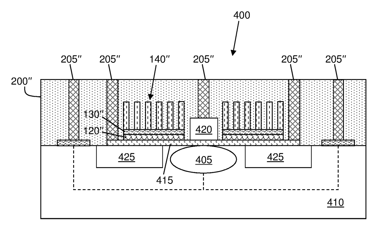
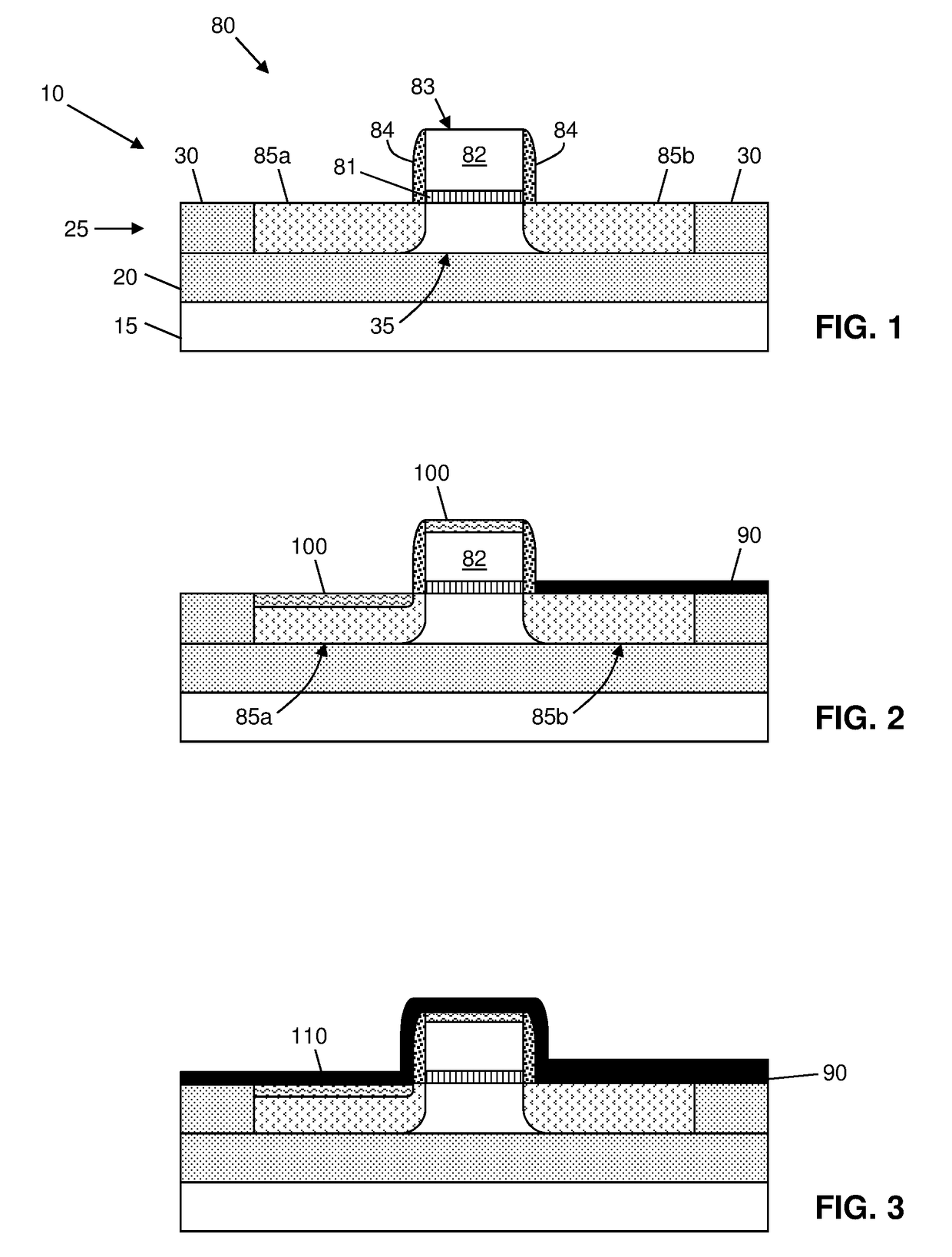
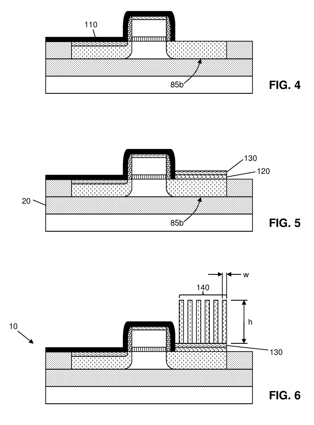
[0013]The invention relates to integrated circuits and, more particularly, to methods and systems for dissipating heat in integrated circuit devices. According to aspects of the invention, nanowire structures are formed to produce an electrically isolated but thermally conductive path for heat to diffuse away from a device. By placing nanowires on and near devices, the nanowires provide a path for heat dissipation and / or heat transport from a source to a sink, and drastically cool the device, which improves device performance. In embodiments, the nanowires comprise zinc oxide (ZnO), which provides the benefit that the nanowires are easily formed with high selectivity via an electrochemical hydrothermal bath. In addition, ZnO has a high thermal conductivity and is a cost-effective, environmentally friendly, and readily available material. Including these nanowire heat fins in devices as described herein provides for further optimization of devices, such as reducing the number of cont...


PUM


Abstract

An approach for heat dissipation in integrated circuit devices is provided. A method includes forming an isolation layer on an electrically conductive feature of an integrated circuit device. The method also includes forming an electrically conductive layer on the isolation layer. The method additionally includes forming a plurality of nanowire structures on a surface of the electrically conductive layer.

Description

FIELD OF THE INVENTION[0001]The present invention relates to integrated circuits and, more particularly, to methods and systems for dissipating heat in integrated circuit devices.BACKGROUND[0002]Silicon-on-insulator is the process of fabricating silicon based devices, such as complementary metal oxide semiconductor (CMOS) field effect transistors (FET) on top of a layer of electrically insulating material, such as an oxide. The layer of oxide is on top of a bulk silicon substrate in an integrated circuit (IC) chip and acts as an electrical barrier between the devices (e.g., FETs) and the bulk silicon. The layer of oxide greatly reduces electrical leakage from the devices, but also greatly reduces heat flow away from these devices. Accumulation of heat within a device, such as a FET, can reduce the performance and / or useful lifetime of the device.[0003]Heat generation is a limiting factor to improving device operation in many technologies. For example, in radio frequency (RF) CMOS, s...

Claims


Application Information

Patent Timeline
Patent Type & Authority Patents(United States)
IPC IPC(8): H01L29/08H01L29/45H01L29/732H01L29/06H01L23/367H01L29/41
CPCH01L23/3677H01L29/0649H01L29/732H01L29/456H01L29/413B82Y10/00H01L29/41725H01L29/0676H01L21/02488H01L21/02554H01L21/02603H01L21/02628H01L2924/0002H01L23/481H01L23/485H01L23/3731H01L29/78H01L23/5256H01L28/20H01L2924/00H01L29/45H01L21/02178H01L21/02189H01L21/02112H01L21/28518H01L21/2855H01L21/28568H01L29/1004H01L29/0821H01L29/0804H01L21/7624H01L29/0665H01L21/02521H01L29/0673H01L29/66242H01L21/4882H01L23/3738H01L21/02271H01L21/2885H01L21/32051H01L21/32053
Inventor BOTULA, ALAN B.LIFSON, MAX L.SLINKMAN, JAMES A.VAN KESSEL, THEODORE G.WOLF, RANDY L.
Owner IBM CORP
Why Eureka
Try Eureka