Defect screening method for electronic circuits and circuit components using power spectrum anaylysis

a technology of power spectrum and defect screening, applied in the direction of resistance/reactance/impedence, measurement devices, instruments, etc., can solve the problems of large failure analysis, high cost, time-consuming, and laborious, and achieve the effect of reducing the number of defects

Active Publication Date: 2018-12-04
NAT TECH & ENG SOLUTIONS OF SANDIA LLC
View PDF11 Cites 5 Cited by
  • Summary
  • Abstract
  • Description
  • Claims
  • Application Information

AI Technical Summary

Benefits of technology

[0007]In a herein-disclosed method for defect screening in an IC or other circuit element, a time-varying signal is supplied to a device sample. The power spectrum of the device sample is measured at one of the pins of the device sample. A defect in the device sample can be identified by comparing the power spectrum with one or more power spectra of the device that have a known defect status.

Problems solved by technology

Therefore, to identify a defect in an IC generally requires extensive failure analysis.
However, these techniques are quite complex, time-consuming, and costly.
Further, an IC can contain a latent defect (also referred to as a “failure precursor”) that is likely to develop into a defect after a period of use.
Conventionally, these latent defects are detected by subjecting the IC to reliability testing, during which the device receives high voltage and / or high temperature for a period of time.
Reliability testing can be quite time-consuming and can significantly increase the production cost.

Method used


Image

  • Defect screening method for electronic circuits and circuit components using power spectrum anaylysis
  • Defect screening method for electronic circuits and circuit components using power spectrum anaylysis
  • Defect screening method for electronic circuits and circuit components using power spectrum anaylysis

Examples


first embodiment

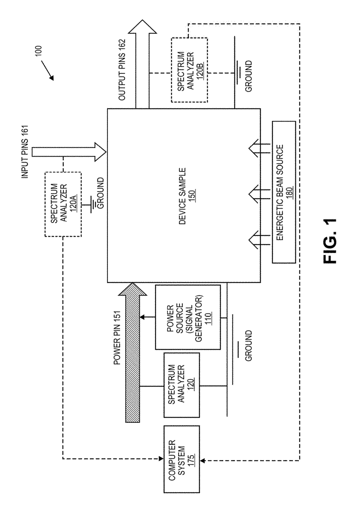
[0037]FIG. 1 is a block diagram illustrating a system 100 for power spectrum analysis (PSA) measurement. In this embodiment, system 100 includes a power source 110 and a spectrum analyzer 120 coupled between a power pin 151 and the ground of a sample of a device (also referred to as “device sample”150). In one embodiment, device sample 150 is a sample of an integrated circuit device. Device sample 150 can be in wafer form (i.e., with multiple other samples of the device on a common semiconductor substrate), in die form (i.e., separated from the wafer but not yet packaged), or in packaged form.

[0038]In the embodiment of FIG. 1, power source 110 is a signal generator that provides a dynamic (i.e., time-varying) stimulus to device sample 150 through its power pin 151. In one embodiment, the input to spectrum analyzer 120 is the same dynamic stimulus that feeds into power pin 151. The dynamic stimulus can be a periodic waveform of ripple voltage, such as sine-wave, square wave, chirp, o...

second embodiment

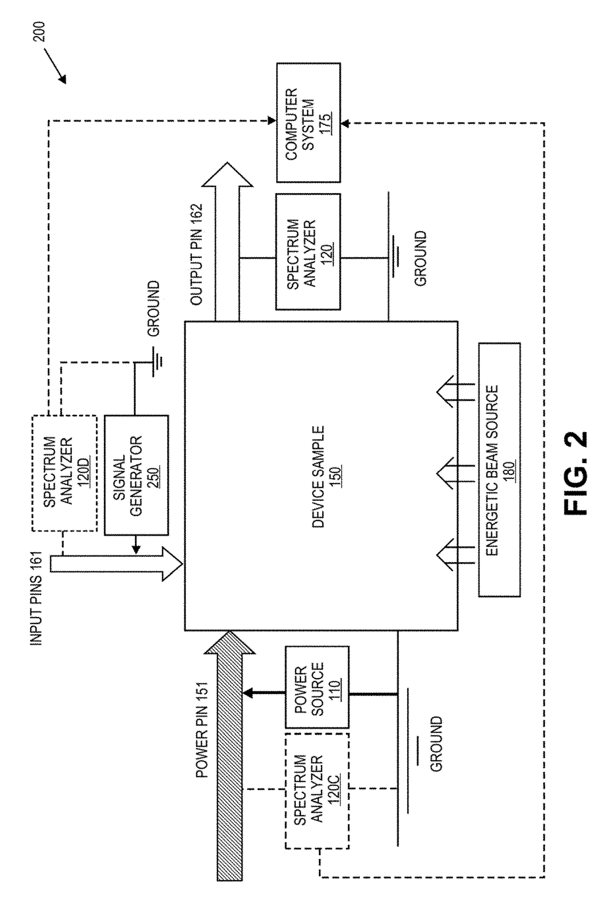
[0042]FIG. 2 is a block diagram illustrating a system 200 for power spectrum analysis (PSA) measurement. In this embodiment, the dynamic stimulus is provided to device sample 150 through at least one of input pins 161. Power source 110 provides voltage, normally constant voltage, to power pin 151, and at least one input pin 161 receives a dynamic stimulus from a signal generator 250. The dynamic stimulus can be a time-varying sequence of voltages (e.g., sine wave, square wave, or a sequence of logical lows and highs). The rest of input pin 161 can be either floating, biased with a constant voltage, or biased with a switching voltage to maintain a known dynamic biasing state. In some embodiments, signal generator 250 may be a vector generator that is coupled to multiple input pins 161 to supply the dynamic stimulus in the form of a sequence of test vectors (with each test vector being a vector of logical lows and highs). These test vectors can also be used for functional testing of d...


PUM


Abstract

A method involving the non-destructive testing of a sample electrical or electronic device is provided. The method includes measuring a power spectrum of the device and performing a Principal Component Analysis on the power spectrum, thereby to obtain a set of principal components of the power spectrum. The method further includes selecting a subset consisting of some of the principal components, and comparing the subset to stored reference data that include representations in terms of principal components of one or more reference populations of devices. Based at least partly on the comparison, the sample device is classified relative to the reference populations.

Description

CROSS-REFERENCE TO RELATED APPLICATIONS[0001]This application is a continuation-in-part of U.S. patent application Ser. No. 13 / 309,281, which was filed on Dec. 1, 2011 by Paiboon Tangyunyong under the title “Power Spectrum Analysis for Defect Screening in Integrated Circuit Devices”, which is commonly owned herewith, and the entirety of which is hereby incorporated herein by reference.FEDERALLY SPONSORED RESEARCH[0002]The United States Government has rights in this invention pursuant to Department of Energy Contract No. DE-AC04-94AL85000 with Sandia Corporation.FIELD OF THE INVENTION[0003]Device testing; and in particular, the use of power spectra for defect screening in integrated circuit devices.ART BACKGROUND[0004]An integrated circuit (IC) can have millions of transistors with a feature size less than a micrometer. Therefore, to identify a defect in an IC generally requires extensive failure analysis. In the past, various techniques based on electrical, optical, and thermal prop...

Claims


Application Information

Patent Timeline
Patent Type & Authority Patents(United States)
IPC IPC(8): G01R31/28G01R27/28
CPCG01R31/2894G01R27/28G01R31/31718G01R23/16G01R31/2851G01R31/31721
Inventor TANGYUNYONG, PAIBOONBEUTLER, JOSHUACOLE, JR., EDWARD I.LOUBRIEL, GUILLERMO M.
Owner NAT TECH & ENG SOLUTIONS OF SANDIA LLC
Why Eureka
Try Eureka