
Light emitting diode chip having temperature compensation of the wavelength

a technology of light-emitting diodes and wavelength compensation, which is applied in the direction of basic electric elements, electrical equipment, semiconductor devices, etc., can solve the problem of increasing the wavelength of emitted radiation with increasing operating temperature, and achieve the effect of reducing the temperature-dependent radiation emission

Active Publication Date: 2019-02-26
OSRAM OLED
View PDF21 Cites 1 Cited by
  • Summary
  • Abstract
  • Description
  • Claims
  • Application Information

AI Technical Summary

Benefits of technology

The emission spectrum remains relatively stable with minimal change in dominant wavelength and perceived brightness, even across temperature variations from 25°C to 85°C, effectively counteracting the temperature-dependent bandgap decrease.

Problems solved by technology

For radiation-emitting optoelectronic semiconductor chips such as LEDs or semiconductor lasers, for example, this can result in the wavelength of the emitted radiation increasing with rising operating temperature.

Method used


Image

  • Light emitting diode chip having temperature compensation of the wavelength
  • Light emitting diode chip having temperature compensation of the wavelength
  • Light emitting diode chip having temperature compensation of the wavelength

Examples


Embodiment Construction

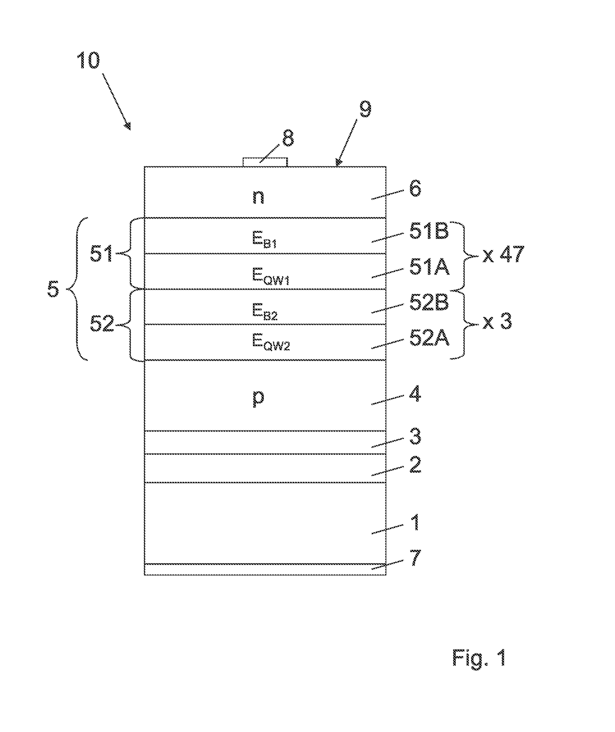
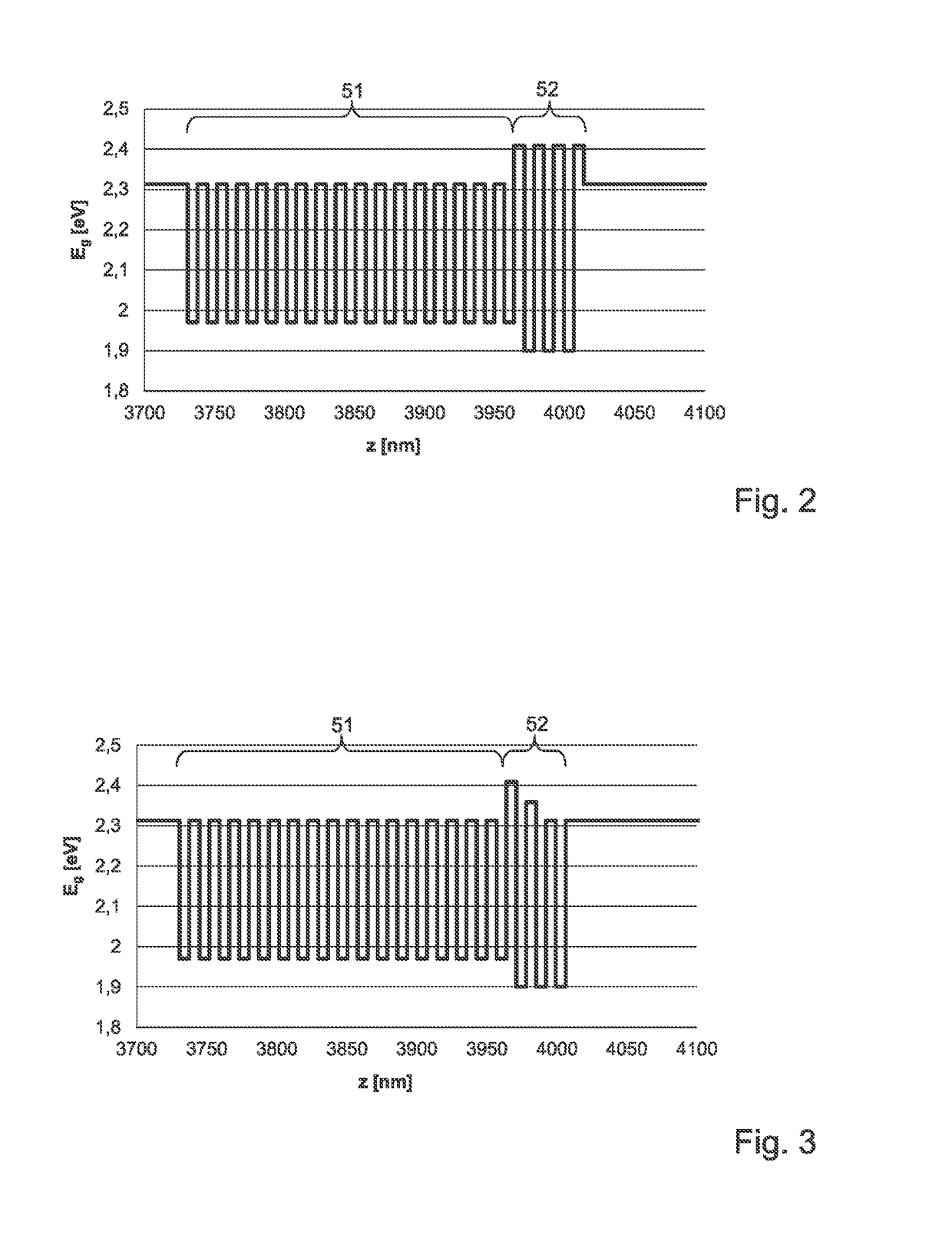
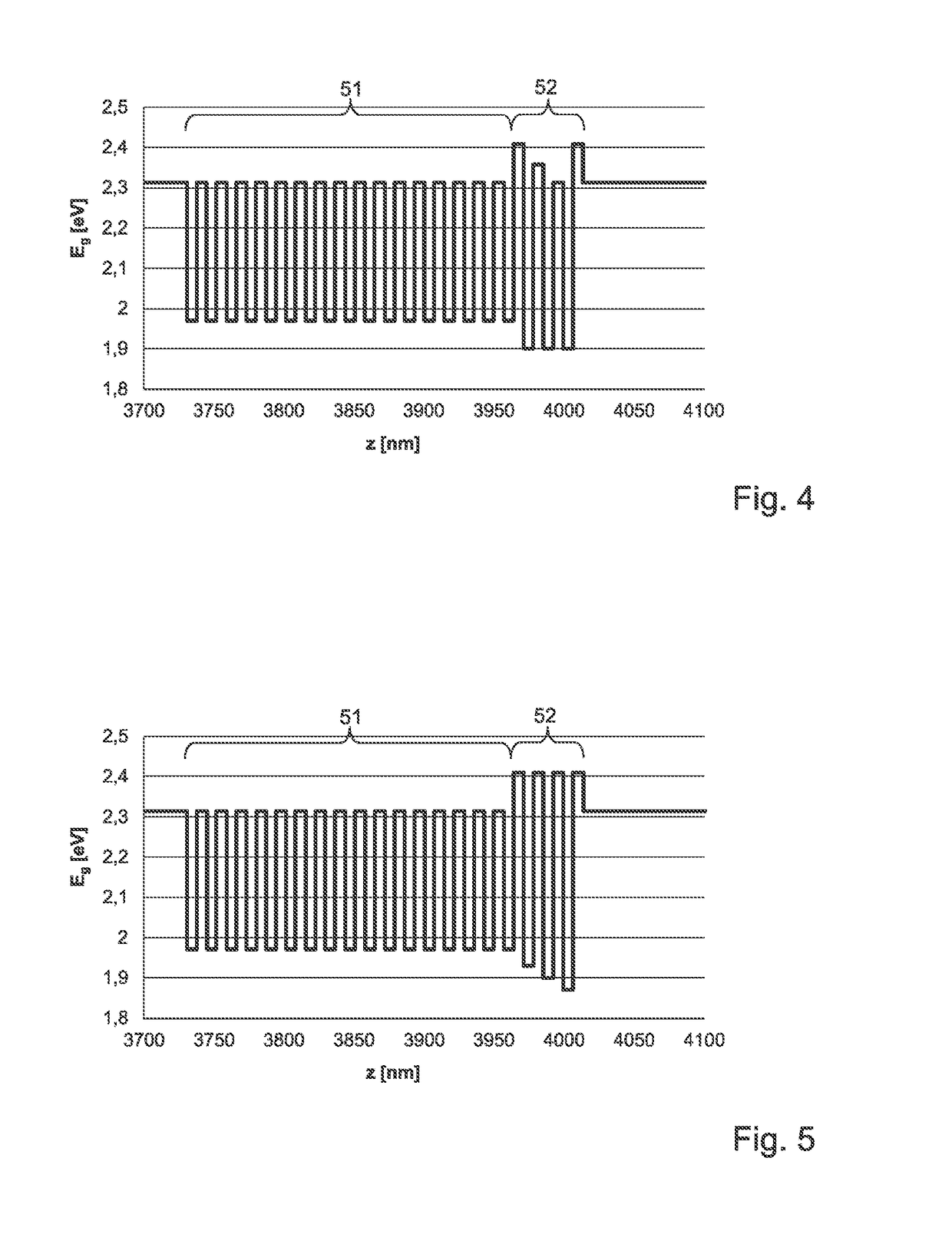
[0025]The optoelectronic semiconductor chip 10 shown in FIG. 1 according to an exemplified embodiment is an LED chip, which comprises a p-type semiconductor region 4, an n-type semiconductor region 6 and an active layer 5, which is arranged between the p-type semiconductor region 4 and the n-type semiconductor region 6 and is adapted for emitting radiation. The exemplified embodiment of the optoelectronic semiconductor chip 10 is what is known as a thin-film semiconductor chip, from which a growth substrate has been removed that was used originally for epitaxial growth of the semiconductor layers 4, 5, 6, and instead the semiconductor layer stack has been bonded by means of a bonding layer 2, in particular a solder layer, to a carrier substrate 1 that is different from the growth substrate.

[0026]In a thin film LED chip 10 of this type, the p-type semiconductor region 4 typically faces the carrier substrate 1. A mirror layer 3, which advantageously deflects radiation emitted towards ...


PUM


Abstract

An optoelectronic semiconductor chip is disclosed. In an embodiment the optoelectronic semiconductor chip includes a p-type semiconductor region, an n-type semiconductor region, and an active layer arranged between the p-type semiconductor region and the n-type semiconductor region. The active layer is designed as a multiple quantum well structure, wherein the multiple quantum well structure has a first region of alternating first quantum well layers and first barrier layers and a second region having at least one second quantum well layer and at least one second barrier layer. The at least one second quantum well layer has an electronic band gap (EQW2) that is less than the electronic band gap (EQW1) of the first quantum well layers, and the at least one second barrier layer has an electronic band gap (EB2) that is greater than the electronic band gap (EB1) of the first barrier layers.

Description

[0001]This patent application is a national phase filing under section 371 of PCT / EP2015 / 077661, filed Nov. 25, 2015, which claims the priority of German patent application 10 2014 117 611.1, filed Dec. 1, 2014, each of which is incorporated herein by reference in its entirety.TECHNICAL FIELD[0002]The invention relates to an optoelectronic semiconductor chip.BACKGROUND[0003]The optical and electronic properties of semiconductor materials are largely determined by the bandgap, i.e., the difference in energy between the valence band and the conduction band. The bandgap of semiconductor materials generally decreases with rising temperature. For radiation-emitting optoelectronic semiconductor chips such as LEDs or semiconductor lasers, for example, this can result in the wavelength of the emitted radiation increasing with rising operating temperature. This can alter the perceived color of the emitted radiation.[0004]It is also known that the sensitivity of the human eye decreases at wav...

Claims


Application Information

Patent Timeline
Patent Type & Authority Patents(United States)
IPC IPC(8): H01L33/06H01L33/08
CPCH01L33/08H01L33/06
Inventor RUDOLPH, ANDREASSUNDGREN, PETRUSTANGRING, IVAR
Owner OSRAM OLED
Learn More