CMOS image sensor having enhanced near infrared quantum efficiency and modulation transfer function

a near infrared and quantum efficiency technology, applied in the field of semiconductor image sensors, can solve the problems of reducing performance, reducing performance, and additional semiconductor thickness, and reducing the efficiency of conventional image sensor devices

Active Publication Date: 2019-03-05
OMNIVISION TECH INC
View PDF8 Cites 1 Cited by
  • Summary
  • Abstract
  • Description
  • Claims
  • Application Information

AI Technical Summary

Benefits of technology

[0057]In FIG. 19A-B, the NIR QE enhancement elements 701 are disposed in the photodiode 702 at the front side surface 706 where the incident light is received through. They are arranged in rows and columns to form a NIR QE enhancement sub-structure 1901a with a rectangle pattern, to modify the incident light at the front side surface 706 by at least one of diffraction, deflection and reflection, to redistribute the incident light within the photodiode 702 to improve optical sensitivity, including NIR light sensitivity, of the image sensor 1900. Moreover, a dielectric material 713 is deposited on the backside surface 705 of the silicon substrate 711, wherein there is an embedded optical reflective layer 712, to form a MTF enhancement sub-structure 1901b. The optical reflective layer 712 would reflect the incident light back into PD 702. More specifically, the optical reflective layer 712 is designed with a geometry substantially corresponding to the NIR QE enhancement sub-structure 1901a in order to ensure the incident light is still within the photodiode 702 even after redistribution, so as to prevent the cross talk between adjacent PDs and enhance MTF consequently. In one example, the optical reflective layer 712 has the same size as the rectangle pattern of NIR QE enhancement sub-structure 1901a, and align up with the edge of the rectangle pattern of the NIR QE enhancement sub-structure 1901a as well. In one example, the optical reflective layer 712 comprises at least one of Au, Cu, Ti, Al, Pt, Ag, Ta, and Al / Cu. In another example, the optical reflective layer 712 comprises a structure which is stacked by several different layers, for example, TiN stacked on the top of Al, TiN stacked on the top of Ti, W stacked on the top of Ti, etc. In one example, the dielectric material 713 comprises organic dielectric materials such as photo resist, and inorganic dielectric materials such as silicon oxide and silicon nitride. In another example, the dielectric material 713 comprises a structure which is stacked by several different layers, for example, silicon nitride stacked on the top of silicon oxide. The thickness of the dielectric material is in a range of 200 Å to 10 μm, and the thickness of the optical reflective layer is in a range of 50 Å to 1 μm.

Problems solved by technology

However, conventional image sensor devices may poorly absorb NIR light due to the band structure of semiconductor materials used in modern microelectronic devices.
Additional semiconductor thickness may complicate other fabrication steps and / or reduce performance.
Furthermore, many materials conductive to absorb NIR light are very expensive (either inherently or by virtue of fabrication techniques needed to process the materials), toxic, and / or have lower sensitivity to the visible spectrum.
Accordingly, many elements / compounds capable of detecting NIR light may not be ideal choices for integration into modern electronic devices.

Method used


Image

  • CMOS image sensor having enhanced near infrared quantum efficiency and modulation transfer function
  • CMOS image sensor having enhanced near infrared quantum efficiency and modulation transfer function
  • CMOS image sensor having enhanced near infrared quantum efficiency and modulation transfer function

Examples


Embodiment Construction

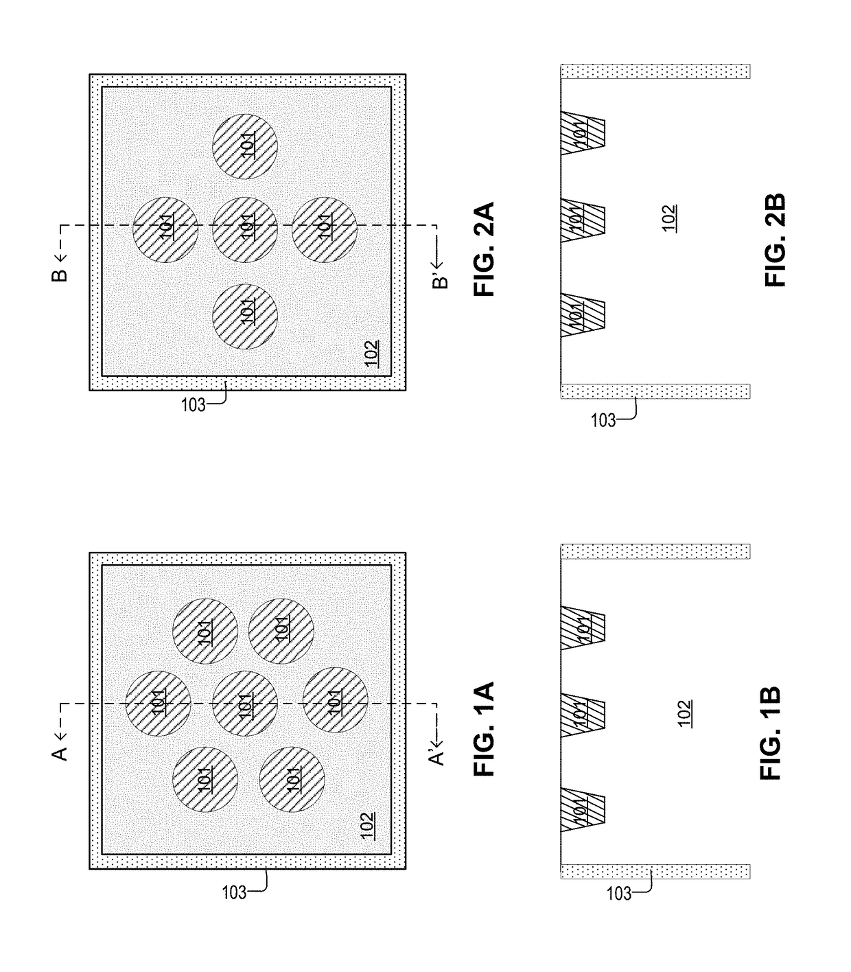
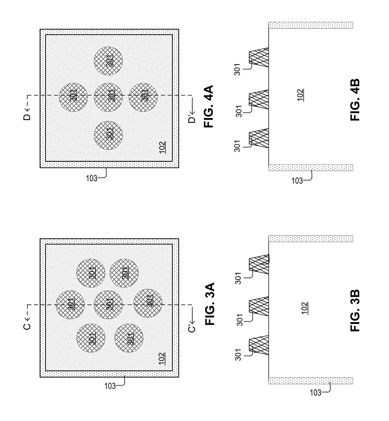
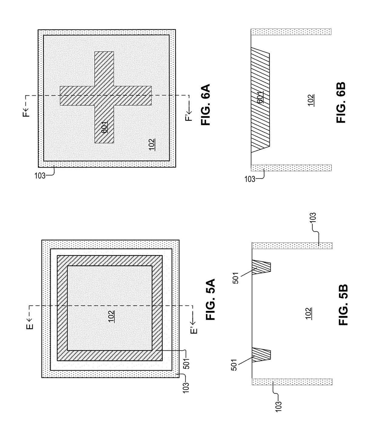
[0033]Examples of an apparatus for an image sensor with enhanced NIR QE and MTF are described herein. In the following description, numerous specific details are set forth to provide a thorough understanding of the examples. However, one skilled in the relevant art will recognize that the techniques described herein can be practiced without one or more of the specific details, or with other methods, components, materials, etc. In other instances, well-known structures, materials, or operations are not shown or described in details in order to avoid obscuring certain aspects.

[0034]Reference throughout this specification to “one example” or “one embodiment” means that a particular feature, structure, or characteristic described in connection with the example is included in at least one example of the present invention. Thus, the appearances of the phrases “in one example” or “in one embodiment” in various places throughout this specification are not necessarily all referring to the sa...


PUM


Abstract

An image sensor comprises a semiconductor material having an illuminated surface and a non-illuminated surface; a photodiode formed in the semiconductor material extending from the illuminated surface to receive an incident light through the illuminated surface, wherein the received incident light generates charges in the photodiode; a transfer gate electrically coupled to the photodiode to transfer the generated charges from the photodiode in response to a transfer signal; a floating diffusion electrically coupled to the transfer gate to receive the transferred charges from the photodiode; and a near infrared (NIR) quantum efficiency (QE) and modulation transfer function(MTF) enhancement structure. The NIR QE and MTF enhancement structure comprises: a NIR QE enhancement sub-structure comprising at least one NIR QE enhancement elements within a photosensitive region of the photodiode, wherein the NIR QE enhancement sub-structure is configured to modify the incident light at the illuminated surface of the semiconductor material by at least one of diffraction, deflection and reflection, to redistribute the incident light within the photodiode to improve optical sensitivity, including NIR light sensitivity, of the image sensor; and a MTF enhancement sub-structure disposed on the non-illuminated surface of the semiconductor material, facing toward the NIR QE enhancement sub-structure, wherein the MTF enhancement structure has a geometry corresponding to the NIR QE enhancement sub-structure, to ensure the incident light is still within the photodiode after redistribution.

Description

CROSS-REFERENCE TO RELATED APPLICATION[0001]This disclosure is a Continuation-in-Part (CIP) Application of U.S. patent application Ser. No. 15 / 642,177, filed on Jul. 5, 2017.TECHNICAL FIELD[0002]This disclosure relates generally to semiconductor image sensors, and in particular but not exclusively, relates to CMOS image sensors having enhanced near infrared (NIR) Quantum Efficiency (QE) and modulation transfer function (MTF).BACKGROUND INFORMATION[0003]Image sensors have become ubiquitous. They are widely used in digital still cameras, cellular phones, security cameras, as well as, medical, automobile, and other applications. The technology used to manufacture image sensors has continued to advance at a great pace. For example, the demands of higher resolution and lower power consumption have encouraged the further miniaturization and integration of these devices.[0004]Detection of near infrared (NIR) light is useful in automotive and night vision applications. However, conventional...

Claims


Application Information

Patent Timeline
Patent Type & Authority Patents(United States)
IPC IPC(8): H04N5/33H04N5/335H01L27/146H01L27/148H04N5/3745
CPCH01L27/14649H01L27/148H01L27/1461H01L27/1463H04N5/3745H01L27/14612H01L27/14629H04N5/332H04N5/335H01L27/1464H01L27/14601H01L27/14603H01L27/14643H04N23/11H04N25/00H04N25/77
Inventor ZHAO, CHENGYANG, CUNYULU, CHEN-WEILIN, ZHIQIANG
Owner OMNIVISION TECH INC
Why Eureka
Try Eureka