
Thermoelectric material, thermoelectric module, optical sensor, and method for manufacturing thermoelectric material

a technology of thermoelectric modules and thermoelectric materials, applied in the direction of thermoelectric device junction materials, thermoelectric device manufacturing/treatment, thermoelectric device with peltier/seeback effect, etc., can solve the problem that the conductivity of the thermoelectric material may be lowered, and achieve excellent thermoelectric characteristics

Active Publication Date: 2019-04-23
SUMITOMO ELECTRIC IND LTD
View PDF25 Cites 0 Cited by
  • Summary
  • Abstract
  • Description
  • Claims
  • Application Information

AI Technical Summary

Benefits of technology

The patent discusses how to create a material using nanostructures that have excellent properties for heating and cooling. This material can be made into a thermoelectric device.

Problems solved by technology

The thermoelectric material, however, may suffer from lowering in conductivity, because an insulator buries a gap between particles.

Method used


Image

  • Thermoelectric material, thermoelectric module, optical sensor, and method for manufacturing thermoelectric material
  • Thermoelectric material, thermoelectric module, optical sensor, and method for manufacturing thermoelectric material
  • Thermoelectric material, thermoelectric module, optical sensor, and method for manufacturing thermoelectric material

Examples


first embodiment

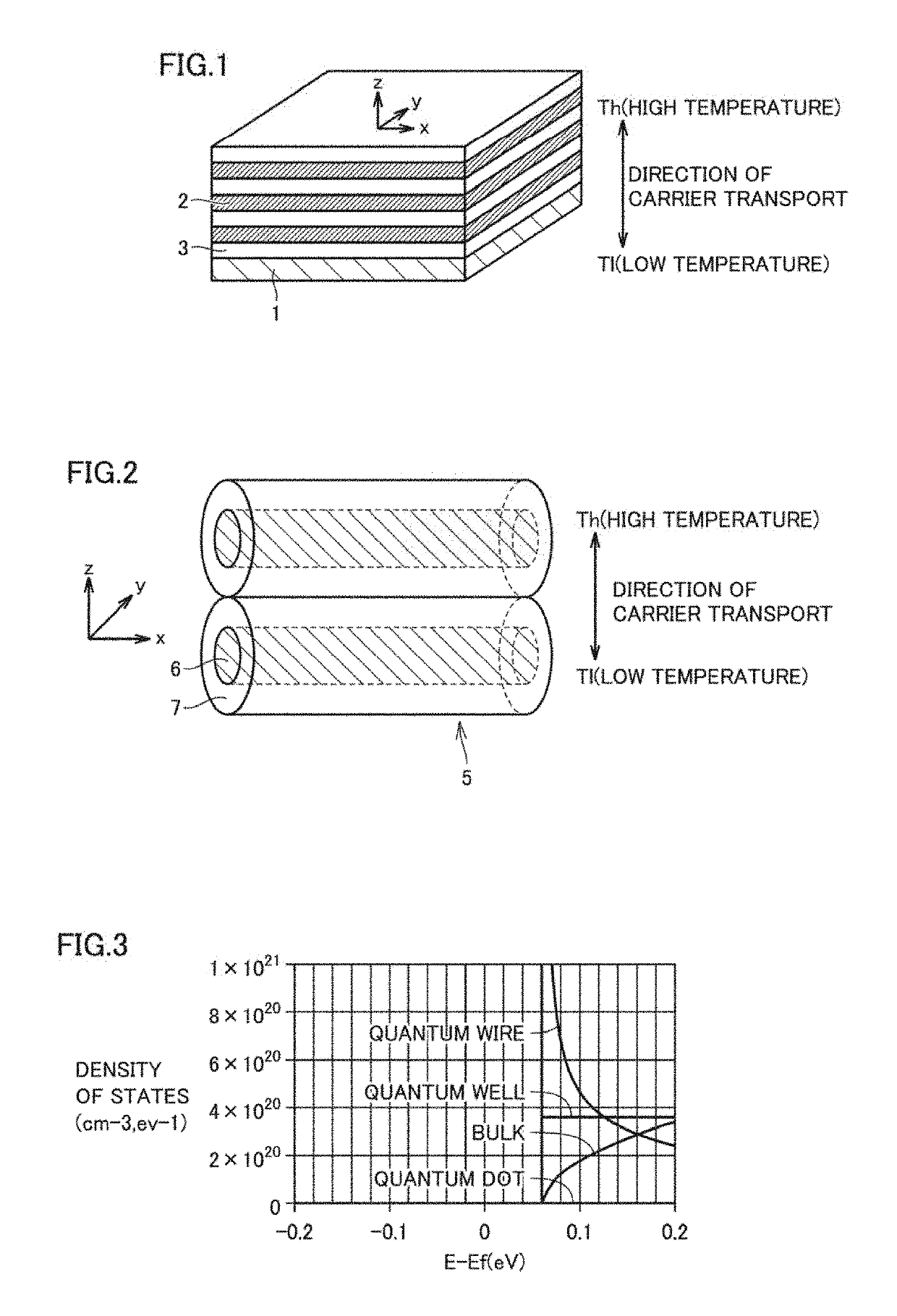
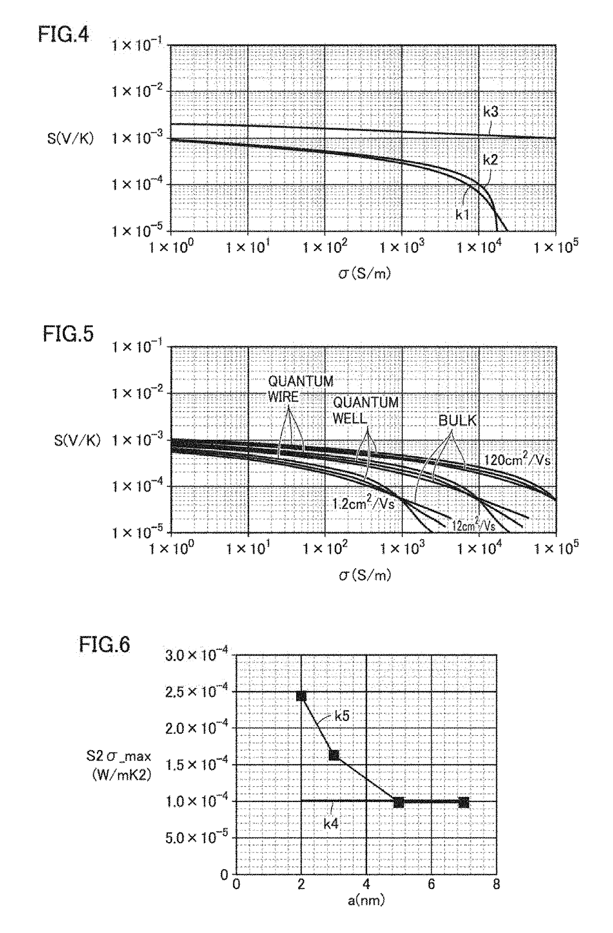
[0080]A basic construction of a thermoelectric material according to this invention will initially be described. FIG. 1 is a perspective view schematically showing a thermoelectric material having a quantum well structure. FIG. 2 is a perspective view schematically showing a thermoelectric material having a quantum wire structure.

[0081]Referring to FIG. 1, a quantum well structure is formed by alternately stacking on a main surface of a substrate 1, two semiconductor layers 2 and 3 different from each other in band gap energy. Since semiconductor layer 2 is relatively low in band gap energy, it forms a quantum well layer. Since semiconductor layer 3 is relatively high in band gap energy, it forms an energy barrier layer.

[0082]The quantum well structure is a structure in which a state that an energy level is discretized can be obtained as an electron state around a valence band and a conduction band is quantized in a one-dimensional direction (for example, in a direction of a thickne...

second embodiment

[0115]In this embodiment, wave functions of carriers are combined between quantum dots by decreasing an interval between quantum dots (nanoparticles). A quantum dot structure is a structure in which a state that an electron state around a valence band and a conduction band is quantized in a three-dimensional direction and an energy level is discretized is obtained. The quantum dot structure can have discrete sub band structures not only in the z direction but also in the x direction and the y direction, and can achieve effective energy conversion. With this quantum effect of the quantum dots, transport of carriers between the quantum dots is allowed. FIG. 10 is a schematic diagram showing a construction of a thermoelectric material 20 according to this invention. In the description below, a quantum dot structure shown in FIG. 10 is also referred to as a “quantum network (net) structure.”

[0116]Referring to FIG. 10, in the quantum net structure, quantum dots (nanoparticles) 30 impleme...

third embodiment

[0162]A method for manufacturing a thermoelectric material according to this invention includes a stacking step of alternately stacking a first layer containing a different element and a second layer not containing the different element and an annealing step of forming nanoparticles in a base material by subjecting a stack of the first layer and the second layer to annealing treatment.

[0163]In the third embodiment, the stacking step is a step of alternately stacking the first layer and the second layer on a substrate body. Such a substrate body is preferably formed in such a manner that an uppermost portion thereof in contact with the first layer or the second layer is formed of a material capable of forming a solid solution of the different element. With such a construction, in diffusion of the different element through annealing treatment, the different element can diffuse also in the substrate body and precipitation of the different element as being concentrated in a specific por...


PUM


Abstract

A thermoelectric material includes a plurality of first semiconductor members having first band gap energy and a second semiconductor member having second band gap energy higher than the first band gap energy. The first semiconductor member and the second semiconductor member are alternately arranged in a direction of carrier transport. The first semiconductor member has a width in the direction of carrier transport not greater than 5 nm and a distance between two adjacent first semiconductor members in the direction of carrier transport is not greater than 3 nm.

Description

TECHNICAL FIELD[0001]This invention relates to a thermoelectric material constituted of nanostructures and a thermoelectric module and an optical sensor including the same, as well as a method for manufacturing a thermoelectric material constituted of nanostructures.BACKGROUND ART[0002]A thermoelectric material converts a temperature difference (thermal energy) into electric energy, and conversion efficiency η thereof is expressed in an expression (1) below.[0003]η=Δ⁢⁢TTh⁢M-1M+TcTh(1)[0004]In the expression (1) above, Th represents a temperature on a high-temperature side, Tc represents a temperature on a low-temperature side, and ΔT represents a temperature difference between Th and Tc (=Th−Tc). M is given in an expression (2) below, using a dimensionless performance index ZT representing an index representing performance of a thermoelectric material. This dimensionless performance index ZT is a value obtained by multiplying a performance index Z by an absolute temperature T, and e...

Claims


Application Information

Patent Timeline
Patent Type & Authority Patents(United States)
IPC IPC(8): H01L35/30H01L35/34H01L35/22H01L35/26H10N10/13H10N10/17H10N10/857H10N10/01H10N10/851H10N10/855
CPCH01L35/26H01L35/22H01L35/34H10N10/857H10N10/855H10N10/01H10N10/8556
Inventor ADACHI, MASAHIROYAMAMOTO, YOSHIYUKI
Owner SUMITOMO ELECTRIC IND LTD
Learn More