Method for forming vertical spacers for spacer-defined patterning

a technology of vertical spacers and patterning, which is applied in the field of forming vertical spacers for spacer-defined patterning, can solve the problems of difficult for semiconductor manufacturers to continuously conduct subsequent integration processes precisely, the problem of increasing the problem of above leaning, and the difficulty of pattern miniaturization in lithography technology

Active Publication Date: 2019-05-14
ASM IP HLDG BV
View PDF2768 Cites 241 Cited by
  • Summary
  • Abstract
  • Description
  • Claims
  • Application Information

AI Technical Summary

Benefits of technology

[0005]In order to solve at least one of the problems in the conventional patterning, in some embodiments of the present invention, the spacers are formed by using a two-layer film, thereby controlling the leaning angle of the etched spacers, particularly inhibiting or suppressing the spacers from inwardly leaning, which angle is defined as an angle of an inner face of each sidewall portion as measured with reference to a line vertical to a bottom of a vacant space which is formed by removing a core material between the spacers, wherein a leaning angle of zero represents completely vertical and a leaning angle of a positive value represents leaning inward. The two-layer film satisfies the conditions that the two layers have different film stresses and both are highly conformal (preferably formed by atomic layer deposition, ALD). By changing the difference in film stress between the two layers, th

Problems solved by technology

However, lithography technology faces difficulties in pattern miniaturization due to the limited wavelength of a laser light used in lithography.
This leaning phenomenon makes it difficult for semiconductor manufacturers to continuously conduct subsequent integration processes precisely.
It is expected that the above leaning problem will become more serious as technology advances and mi

Method used


Image

  • Method for forming vertical spacers for spacer-defined patterning
  • Method for forming vertical spacers for spacer-defined patterning
  • Method for forming vertical spacers for spacer-defined patterning

Examples


reference example 1

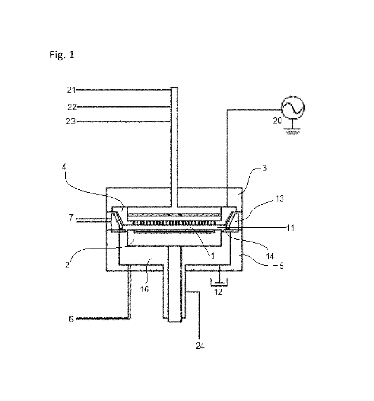
[0108]SiO films and SiN films were each deposited on a Si substrate (0300 mm) by PEALD, one cycle of which was conducted under the conditions shown in Tables 6 and 7 (deposition cycle) below using the PEALD apparatus illustrated in FIG. 1 based on the process sequence illustrated in FIGS. 16 and 17.

[0109]After taking out each substrate from the reaction chamber, film stress of each film was measured. The results are shown in Table 8 below. The film stress was measured based on a “warp” of the substrate before and after the film was deposited on the substrate, wherein the “warp” was expressed by a radius of curvature, and the film stress was calculated using the Stoney equation.

[0110]

TABLE 6(numbers are approximate)Conditions for Deposition Cycle of Silicon Oxide FilmCycle ASubstrate temperature100° C.Pressure400 PaPrecursorBDEAS (bisdiethyl-aminosilane)Precursor pulse (“Feed 1”)0.8 secPrecursor purge (“Purge 1”)2.0 secFlow rate of oxygen (continuous)2 slmFlow rate of Ar (continuous)...

example 1

[0121]A template was prepared and a SiO film was deposited in a manner substantially similar to that in Comparative Example 1 or 2 except that the SiO film was deposited as a SiO two-layer pattern-transfer film which was constituted by an inner SiO single-layer film having a thickness of 20 nm deposited in a manner substantially similar to that in Comparative Example 1 (SiO (n=0)), and an outer SiO single-layer film having a thickness of 15 nm deposited in a manner substantially similar to that in Comparative Example 2 (SiO (n=3)). The SiO two-layer pattern-transfer film had a conformality of 90%. (c) in FIG. 9 shows a STEM photograph of a cross-sectional view of the SiO two-layer film. That is, the inner layer having a thickness of 20 nm was the SiO single-layer film having a stress of −10.7 MPa (relatively tensile), whereas the outer layer having a thickness of 15 nm was the SiO single-layer film having a stress of −169.3 MPa (relatively compressive).

[0122]Next, the SiO two-layer ...

example 2

[0123]A template was prepared and a SiO film was deposited in a manner substantially similar to that in Example 1 except that the inner layer and the outer layer were switched. That is, the SiO film was deposited as a SiO two-layer pattern-transfer film which was constituted by an inner SiO single-layer film having a thickness of 20 nm deposited in a manner substantially similar to that in Comparative Example 2 (SiO (n=3)), and an outer SiO single-layer film having a thickness of 15 nm deposited in a manner substantially similar to that in Comparative Example 1 (SiO (n=0)). The SiO two-layer pattern-transfer film had a conformality of 95%. (e) inFIG. 9 shows a STEM photograph of a cross-sectional view of the SiO two-layer film. That is, the inner layer having a thickness of 20 nm was the SiO single-layer film having a stress of −169.3 MPa (relatively compressive), whereas the outer layer having a thickness of 15 nm was the SiO single-layer film having a stress of −10.7 MPa (relative...


PUM


Abstract

A method of forming vertical spacers for spacer-defined multiple patterning, includes: depositing a first conformal pattern-transfer film having a first film stress, and continuously depositing a second conformal pattern-transfer film having a second film stress on a template; dry-etching the template except for a core material and a vertical portion of the first and second pattern-transfer films to form vertical spacers; and dry-etching the core material, forming a vacant space between the vertical spacers, wherein by adjusting the difference in film stress between the first and second pattern-transfer films, the leaning angle of the spacers is adjusted.

Description

BACKGROUNDField of the Invention[0001]The present invention relates generally to a method for forming vertical spacers for spacer-defined patterning in semiconductor fabrication processes.Related Art[0002]Patterning processes using lithography technology are essential to semiconductor fabrication processes. However, lithography technology faces difficulties in pattern miniaturization due to the limited wavelength of a laser light used in lithography. One approach to realize pattern miniaturization using known patterning technology is SADP (Self Aligned Double Pattering) or SDDP (Spacer-Defined Double Patterning). FIG. 4 is a schematic representation of double patterning (steps (a) to (c)) according to a comparative example. In step (a), mandrels (photoresist) 101 are patterned as a core material on an underlying layer 102. In step (b), a film 103 is deposited to cover the exposed surfaces of the mandrels 101 and the exposed surface of the underlying surface 102 in their entirety. In...

Claims


Application Information

Patent Timeline
IPC IPC(8): H01L21/308H01L21/311H01L21/3213H01L21/033H01L29/66
CPCH01L21/3086H01L21/3088H01L21/31144H01L21/32139H01L21/3081H01L21/0337H01L21/32137H01L29/6656H01L21/0338H01L21/31122H01L21/027H01L21/02274H01L21/31116H01L21/02214H01L21/02219H01L21/76816G03F7/161G03F7/2022
Inventor KUBOTA, TOMOHIROSUSA, YOSHIO
Owner ASM IP HLDG BV
Why Eureka
Try Eureka