Lightweight bistable PUF circuit

Active Publication Date: 2019-10-01
NINGBO UNIV
View PDF7 Cites 6 Cited by
  • Summary
  • Abstract
  • Description
  • Claims
  • Application Information

AI Technical Summary

Benefits of technology

The invention provides a lightweight, bistable PUF circuit that has a reset function, small circuit area, low power consumption, small time delay and high speed. Compared to prior art, the invention has the advantages of a simplified circuit structure, compact layout, and low power consumption. The weak PUF circuit uses a decoding circuit, timing control circuit, and PUF cell array with a unique structure. Each PUF cell is formed by four PMOS transistors, and there is no stack effect among them. The evaluation and data reading stages are integrated, reducing the output response time. Overall, the invention provides a highly efficient and compact PUF circuit with low power consumption, small time delay and high speed.

Problems solved by technology

However, the weak PUF circuit implemented with the SRAM-PUF cell in Document 1 has the following drawbacks: first, keys generated after the SRAM-PUF cell is powered on cannot be reset; second, the SRAM-PUF cell includes six MOS transistors (two PMOS transistors and four NMOS transistors), and thus, too many MOS transistors are adopted; in order to ensure normal reading and writing of the SRAM-PUF cell, the six MOS transistors should be logically in proportion, and consequentially, the minimum process dimension is unavailable for the MOS transistors; and because the six MOS transistors include both PMOS transistors and NMOS transistors, the weak PUF circuit implemented with the SRAM-PUF cell has a large circuit area and high power consumption.

Method used


Image

  • Lightweight bistable PUF circuit
  • Lightweight bistable PUF circuit
  • Lightweight bistable PUF circuit

Examples


embodiment 1

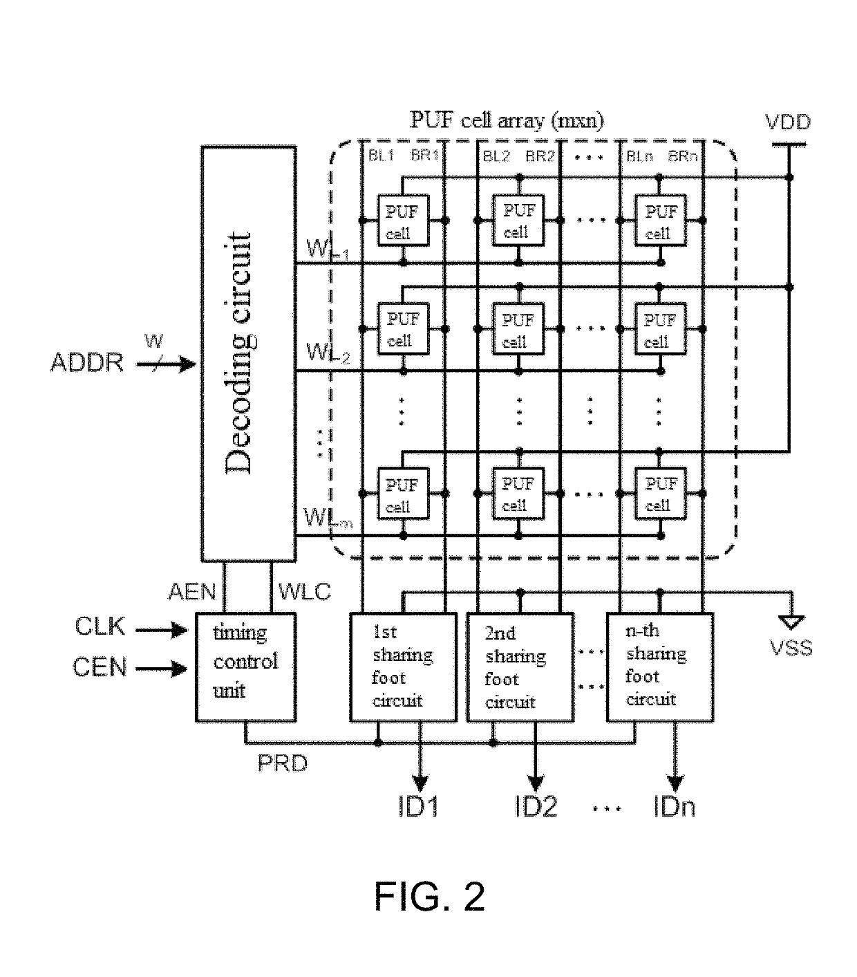
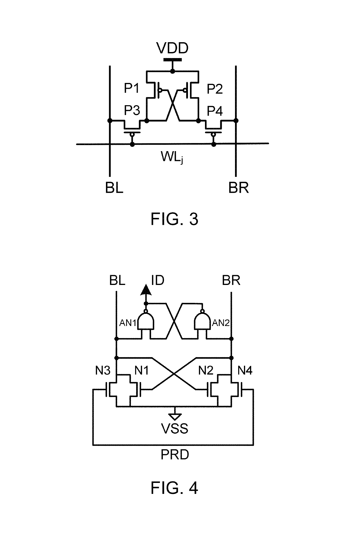
[0024] As shown in FIGS. 2, 3 and 4, a lightweight bistable PUF circuit comprises a decoding circuit, a timing control circuit, a PUF cell array and n sharing foot circuits identical in structure. The PUF cell array is formed by m*n PUF cells which are identical in structure and arrayed in m lines and n columns, wherein * is a multiplication operator. The decoding circuit has w input terminals, m output terminals, a controlled clock signal input terminal and a word line control signal input terminal. The timing control circuit has an enable signal input terminal, a clock signal input terminal, a pre-discharge signal output terminal, a controlled clock signal output terminal and a word line control signal output terminal. Each sharing foot circuit has a pre-discharge signal input terminal, an output terminal, a first bit line connecting terminal and a second bit line connecting terminal. Each PUF cell has a word line connecting terminal, a first bit line connecting terminal and a sec...

embodiment 2

[0027] this embodiment is basically identical with embodiment 1 and is different from embodiment 1 in the following aspects:

[0028]In this embodiment, as shown in FIG. 5, the timing control circuit comprises a latch LH1, a first two-input AND gate A1, a delay chain, a second two-input AND gate A2 and a buffer BF1. The latch LH1 has a clock terminal, an input terminal and an output terminal. The first two-input AND gate A1 and the second two-input AND gate A2 each have a first input terminal, a second input terminal and an output terminal. The input terminal of the latch LH1 is the enable signal input terminal of the timing control circuit. The clock terminal of the latch LH1 is connected to the second input terminal of the first two-input AND gate A1, and a corresponding connecting terminal is the clock signal input terminal of the timing control circuit. The output terminal of the latch LH1 is connected to the first input terminal of the first two-input AND gate A1. The output termi...


PUM


Abstract

Disclosed is a lightweight bistable PUF circuit, comprising a decoding circuit, a timing control circuit, a PUF cell array and n sharing foot circuits. The PUF cell array is formed by m*n PUF cells arrayed in m lines and n columns. Each PUF cell includes a first PMOS transistor, a second PMOS transistor, a third PMOS transistor and a fourth PMOS transistor, and the four PMOS transistors have the minimum width-to-length ratio of 120 nm / 60 nm under a TSMC 65 nm process. Each sharing foot circuit includes a first NMOS transistor, a second NMOS transistor, a third NMOS transistor, a fourth NMOS transistor, a first two-input NAND gate and a second two-input NAND gate, and the four NMOS transistors have a width-to-length ratio ranging from 2 um / 60 nm to 8 um / 60 nm. The lightweight bistable PUF circuit has a reset function and the advantages of small area, low power consumption, small time delay and high speed.

Description

CROSS-REFERENCE TO RELATED APPLICATION[0001]This application claims the priority benefit of China application serial no. 201811207852.2, filed on Oct. 17, 2018. The entirety of the above-mentioned patent application is hereby incorporated by reference herein and made a part of this specification.TECHNICAL FIELD[0002]The invention relates to a PUF circuit, in particular to a lightweight bistable PUF circuit.DESCRIPTION OF RELATED ART[0003]Physical unclonable functions (PUF) can physically guarantee the information security of chips and thus are drawing more and more attentions. PUF circuits are extremely promising embedded key generation circuits which are able to generate a series of random, unique and unclonable output keys by capturing random process deviations of PUF cells, and these output keys can be applied to the information security field for key generation, equipment certification, IP protection and the like.[0004]Nowadays, there are generally two types of PUF circuits, wea...

Claims


Application Information

Patent Timeline
IPC IPC(8): H03K19/003G06F1/10G06F21/75
CPCG06F1/10G06F21/75H03K19/00315G06F21/73
Inventor WANG, PENGJUNLI, GANGZHANG, HUIHONGZHANG, YUEJUN
Owner NINGBO UNIV
Why Eureka
Try Eureka