Method of atomic layer etching using hydrogen plasma

a technology of hydrogen plasma and atomic layer, which is applied in the direction of basic electric elements, semiconductor/solid-state device manufacturing, electric devices, etc., can solve the problems of poor in-plane uniformity of etching of film on a substrate by ale, inability to achieve good in-plane uniformity of etching, and suffer from in-plane uniformity. etching, the effect of high selectivity

Active Publication Date: 2019-12-10
ASM IP HLDG BV
View PDF2891 Cites 5 Cited by
  • Summary
  • Abstract
  • Description
  • Claims
  • Application Information

AI Technical Summary

Benefits of technology

[0009]In some embodiments, when the etchant film deposited on the surface of the target layer is etched by reactive ions such as hydrogen plasma, the components of the etchant film are dissociated and reacted with the reactive ions, generating reactive etchant species which can etch a portion of the target layer at a boundary between the etchant film and the target layer. In the above, only a certain thickness of the etchant film at the boundary can contribute to etching reaction of the target layer because the reactive etchant species need to be generated in a vicinity of the boundary. Further, since the reactive ions which etch the etchant film do not etch the target layer, when the etchant film is removed by the reactive ions, the etching reaction of the target layer stops. Thus, by the above method, a constant amount of the target layer can always be etched by one etching cycle, and thus, controllability and operability of the etching processes are high.
[0012]In some embodiments, the target layer can be constituted by any material (e.g., SiO2, TiO2) which can be etched using a hydrogen halide derived from a CF film. The above etching has high selectivity as to the material constituting the target layer, and thus, for example, a film constituted by silicon or metal oxide can be selectively etched without substantially etching a film constituted by silicon or metal nitride or carbide. In some embodiments, the target layer can be constituted by a material which can be etched using a halogen other than fluorine, as long as a suitable etchant film is selected. Typically, the etchant film is exposed to an oxygen plasma in a reactive ion etching (RIE) process. Since the etching process involves a self-limiting reaction process (or saturation process), high controllability can be realized.

Problems solved by technology

However, it is revealed that in-plane uniformity of etching of a film on a substrate by ALE is not satisfactory when etching an oxide mineral film such as silicon oxide film.
However, when etching a silicon oxide film by ALE using a fluorocarbon such as C4F8 as an etchant gas, good in-plane uniformity of etching is not obtained.
As a result, in-plane uniformity of etching suffers.
However, none of conventional etchant gases satisfies the above.
Similarly, the depth of the etched portion of the target layer increases as the duration of exposure of the etchant film to the plasma increases; however, the depth of the etched portion reaches a plateau and no longer increases when the duration of exposure of the etchant film to the plasma reaches a certain value.

Method used


Image

  • Method of atomic layer etching using hydrogen plasma
  • Method of atomic layer etching using hydrogen plasma

Examples


example 1 (

Prophetic Example)

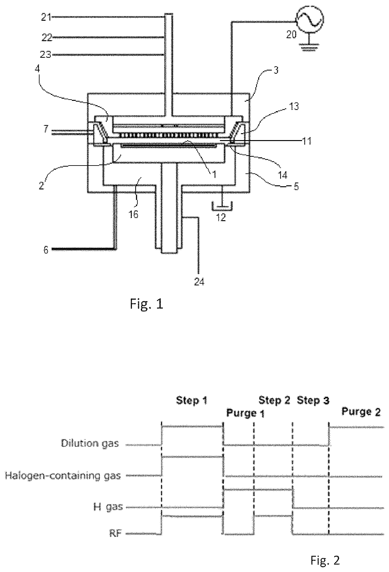
[0059]A silicon oxide film, silicon nitride film, and silicon carbide film are formed at a thickness of about 20 nm by PEALD or PECVD as a target layer on 300-mm substrates, respectively. Deposition of an etchant film (CF film) and etching of each target layer are conducted under the conditions shown in Table 3 below using the plasma-assisted etching apparatus illustrated in FIG. 1. The sequence used in each etching cycle is shown in FIG. 2.

[0060]

TABLE 3(numbers are approximate)Conditions for deposition (PECVD)Substrate temperatureRoom temperaturePressure2.0 PaDeposition gasC2F6Noble gas (as a dilution gas)ArFlow rate of deposition gas10 sccm(etchant gas) (continuous)Flow rate of dilution gas2000 sccm(continuous)RF power for a 300-mm wafer100 W; 13.56 MHz (or 27 MHz,6 MHz, or microwaves)Duration of “RF” (Step 1)2.0 sec.Distance between electrodes30 mmGrowth rate per cycle (nm / cycle)0.7 nm / cycFilm thickness (nm)2.0 nmConditions for etchingSubstrate temperatureSame a...


PUM


Abstract

A method for etching a target layer on a substrate by a dry etching process includes at least one etching cycle, wherein an etching cycle includes: depositing a carbon halide film using reactive species on the target layer on the substrate; and etching the carbon halide film using a plasma of a non-halogen hydrogen-containing etching gas, which plasma alone does not substantially etch the target layer, thereby generating a hydrogen halide as etchant species at a boundary region of the carbon halide film and the target layer, thereby etching a portion of the target layer in the boundary region.

Description

CROSS-REFERENCE TO RELATED APPLICATION[0001]This Application claims priority to U.S. Provisional Patent Application No. 62 / 512,991, entitled “METHOD OF ATOMIC LAYER ETCHING USING HYDROGEN PLASMA,” filed May 31, 2017, the disclosure of which is hereby incorporated herein by reference.BACKGROUND[0002]Field of the Invention[0003]The present invention generally relates to a method of cyclic dry etching of a layer constituted by silicon or metal oxide, for example.[0004]Description of the Related Art[0005]Atomic layer etching (ALE) is cyclic, atomic layer-level etching using an etchant gas adsorbed on a target film and reacted with excited reaction species, as disclosed in Japanese Patent Laid-open Publication No. 2013-235912 and No. 2014-522104. As compared with conventional etching technology, ALE can perform precise, atomic layer-level continuous etching on a sub-nanometer order to form fine, narrow convex-concave patterns and may be suitable for, e.g., double-patterning processes. As...

Claims


Application Information

Patent Timeline
Patent Type & Authority Patents(United States)
IPC IPC(8): H01L21/311H01L21/3065H01L21/306H01L21/3213H01L21/02
CPCH01L21/30621H01L21/32136H01L21/02112H01L21/31122H01L21/02274H01L21/3065H01L21/31116H01L21/30655H01L21/0228
Inventor ZAITSU, MASARUKOBAYASHI, NOBUYOSHIKOBAYASHI, AKIKOHORI, MASARUTSUTSUMI, TAKAYOSHI
Owner ASM IP HLDG BV
Why Eureka
Try Eureka