Deep junction electronic device and process for manufacturing thereof

a technology of deep junction and electronic device, which is applied in the direction of semiconductor/solid-state device manufacturing, basic electric elements, electric apparatus, etc., can solve the problems of inability to apply the technique for forming a deep doped buffer layer on the backside of an ic, and the thermal budget of a processing step of several minutes in an oven at a temperature of more than 1000° c. is extremely high, and achieves low thermal budget

Active Publication Date: 2020-02-18
LASER SYST & SOLUTIONS OF EURO
View PDF1 Cites 0 Cited by
  • Summary
  • Abstract
  • Description
  • Claims
  • Application Information

AI Technical Summary

Benefits of technology

[0014]Therefore one object of the invention is to provide a low thermal budget technique for forming a deep doped buffer layer on the backside of an integrated circuit.
[0026]Furthermore, this process enables better control of the doping level and doping profile. It enables forming a doped layer having a dopant profile which is not achievable using prior art methods.
[0027]As a result, this process enables forming a deep buffer layer of doped monocrystalline semiconductor material at a low thermal budget.
[0030]The process of the present disclosure provides a better control of the profile of a deep doped buffer layer.

Problems solved by technology

For instance, the thermal budget for a processing step of several minutes in an oven at a temperature of more than 1000° C. is extremely high, and incompatible with backside processing.
However, this technique cannot be applied for forming a deep doped buffer layer on the backside of an IC, because thermal diffusion exposes the frontside of the sample to a high temperature and because its long duration (minutes or hours) turns into high thermal budget.
However, high energy implantation is expensive and strongly dependent on the dopant element.
Moreover, laser thermal annealing, which is generally performed at low thermal budget, is limited to the activation of some dopant elements with a limited and specie-dependent diffusion.

Method used


Image

  • Deep junction electronic device and process for manufacturing thereof
  • Deep junction electronic device and process for manufacturing thereof
  • Deep junction electronic device and process for manufacturing thereof

Examples


first embodiment

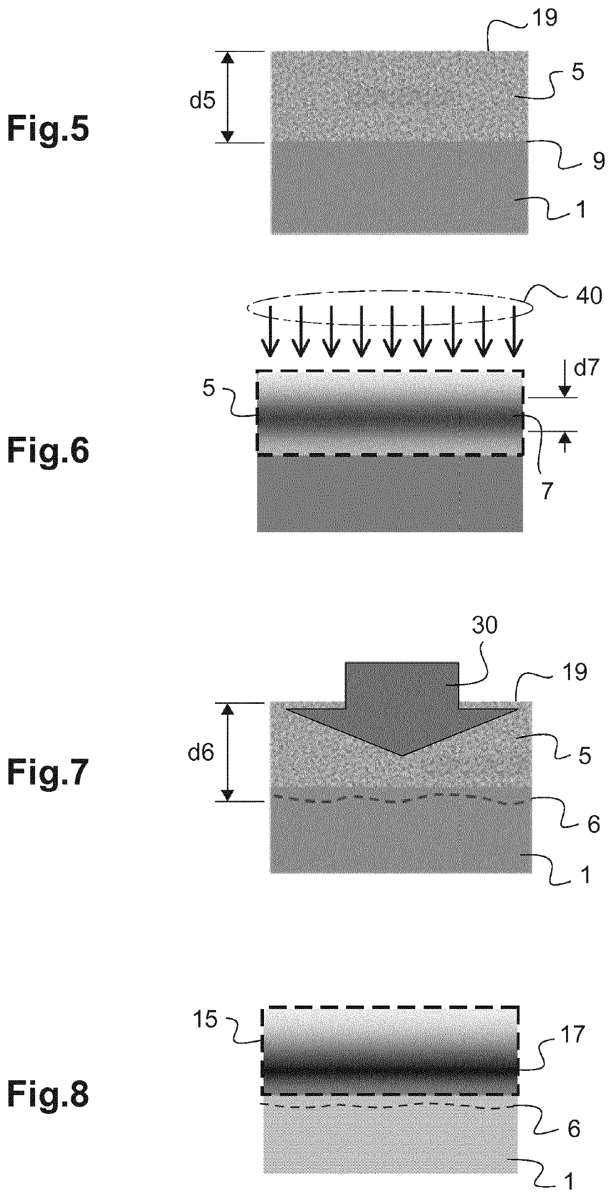
[0073]FIGS. 5 to 7 illustrate a process for forming a doped buried layer according to a first embodiment, and FIG. 8 illustrates the resulting structure.

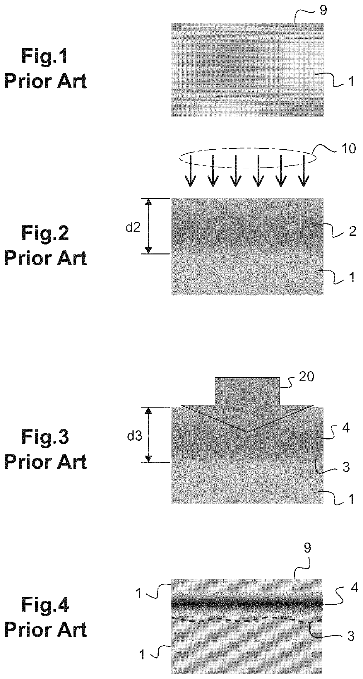
[0074]Prior to the steps illustrated on FIGS. 5 to 7, a monocrystalline semiconductor substrate 1 having a plane surface 9 is provided (as illustrated on FIG. 1). The monocrystalline semiconductor substrate 1 is for example a crystalline silicon (c-Si) substrate or a crystalline germanium (c-Ge) substrate. The plane surface 9 is for instance obtained by chemical mechanical polishing or any other known technique. The plane surface 9 has a determined crystallographic orientation, for example (111) or (100).

[0075]FIG. 5 illustrates a step of deposition of a layer 5 of non monocrystalline semiconductor material on the plane surface 9 of the monocrystalline semiconductor substrate 1. The semiconductor material of the layer 5 and of the substrate 1 have same crystalline lattice. Preferably, the layer 5 and the substrate 1 are made of a sa...

second embodiment

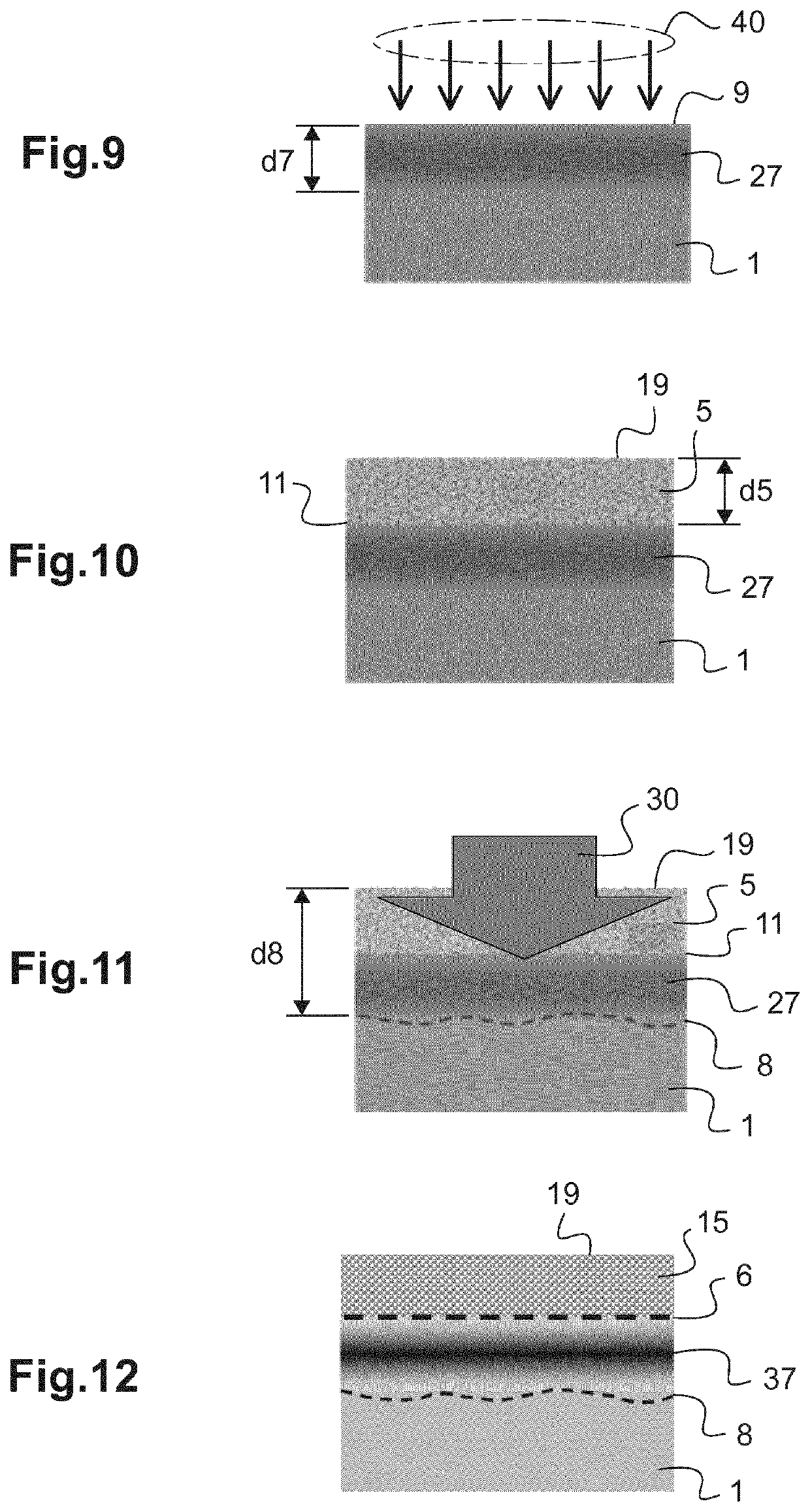
[0094]FIGS. 9 to 11 illustrate a process for forming a doped buried layer according to a second embodiment, and FIG. 12 illustrates the resulting structure.

[0095]Prior to the steps illustrated on FIGS. 9 to 11, a monocrystalline semiconductor substrate 1 having a plane surface 9 is provided (as represented on FIG. 1).

[0096]On FIG. 9, a standard energy implanter is used for implanting dopant ions in a monocrystalline substrate 1. As an example known in the art, phosphorus ions are implanted for generating n type doping or boron ions are implanted for generating n type doping in silicon. An ion implant beam 40 is directed on the back surface 9 of the substrate 1. Preferably, the surface 9 is flat and polished. Dopant species are implanted in the monocrystalline substrate 1 thus forming a layer 27 of monocrystalline semiconductor material including inactivated dopant elements. The layer 27 has a thickness d7 comprised between few hundreds nanometer (i.e. 500 nm) and few micrometers (i....

third embodiment

[0105]A third embodiment consists in a combination of the first and second embodiments. In a first step of the third embodiment, similar to the description in relation with FIG. 9, standard energy implantation is applied to a flat surface 9 of a monocrystalline substrate 1 for implanting dopant elements in the substrate, thus forming a layer 27 of monocrystalline semiconductor material with inactivated doped elements of a first doping type. Then, a layer 5 of non monocrystalline semiconductor material is deposited on the flat surface 9 of the substrate 1. In this third embodiment, the layer 5 may be intrinsic, undoped or doped with inactivated dopant elements of the same doping type or a second doping type. This doping of layer 5 may be performed during deposition of the layer 5 or using another standard energy implantation step, after deposition of the layer 5 (as illustrated on FIG. 6).

[0106]Then, a laser thermal anneal beam 30 is applied to the external surface 19 of the layer 5 ...


PUM

PropertyMeasurementUnit
thicknessaaaaaaaaaa
thicknessaaaaaaaaaa
temperatureaaaaaaaaaa

Abstract

Disclosed is a process for manufacturing a deep junction electronic device including steps of: b) Depositing a layer of non-monocrystalline semiconductor material on a plane surface of a substrate of a monocrystalline semiconductor material; c) Incorporating inactivated dopant elements prior to step b) into said substrate (1) and / or, respectively, during or after step b) into said layer, so as to form an inactivated doped layer; d) Exposing, an external surface of the layer formed at step b) to a laser thermal anneal beam, so as to melt said layer down to the substrate and so as to activate said dopant elements incorporated at step c); e) Stopping exposure to the laser beam so as to induce epi-like crystallization of the melted layer, so that said substrate and / or, respectively, an epi-like monocrystalline semiconductor material, comprises a layer of activated doped monocrystalline semiconductor material.

Description

TECHNICAL FIELD OF THE INVENTION[0001]The invention relates to a method for manufacturing integrated circuits (ICs) comprising a deep electronic junction.[0002]More precisely the invention relates to a device and a method for forming a buffer layer in a deep electronic junction device at a low thermal budget.BACKGROUND INFORMATION AND PRIOR ART[0003]Deep junction devices are used in particular for manufacturing vertical power devices such as IGBT (Insulated Gate Bipolar Transistor) or power metal-oxide-semiconductor field-effect transistor (MOS also MOSFET, MOS-FET, or MOS FET).[0004]Numerous documents describe devices and methods for forming deep electronic junction devices. IC fabrication is achieved by completing first the front-side processing steps and then pursuing with the backside processing steps. The front-side processing is the first portion of IC fabrication where a first part of the deep junction devices is patterned on the front side of a semiconductor wafer, and the b...

Claims


Application Information

Patent Timeline
Patent Type & Authority Patents(United States)
IPC IPC(8): H01L21/02H01L21/268H01L21/265
CPCH01L21/268H01L21/0257H01L21/2652H01L21/02381H01L21/02532H01L21/02675H01L21/26513H01L21/324
Inventor MAZZAMUTO, FULVIO
Owner LASER SYST & SOLUTIONS OF EURO
Why Eureka
Try Eureka