
Semiconductor structure with capacitor landing pad and method of make the same

a capacitor and landing pad technology, applied in the direction of semiconductor devices, semiconductor/solid-state device details, electrical apparatus, etc., can solve the problems of low error margin, unaligned situation at exposure step used, and often occurring location of capacitor landing pads, etc., to increase the contact area therebetween and facilitate short circuit

Active Publication Date: 2020-03-17
UNITED MICROELECTRONICS CORP +1
View PDF11 Cites 0 Cited by
  • Summary
  • Abstract
  • Description
  • Claims
  • Application Information

AI Technical Summary

Benefits of technology

The present invention provides a better way to make the part of a computer chip called a DRAM cell. This new method solves problems that occurred in previous manufacturing processes. The new method uses a reverse tone method to create a cavity in the part of the chip where the metal used to make the connection will be located. This method also creates a specific shape in the part of the chip where the connection will be located, which improves the accuracy of aligning the parts of the chip and reduces the likelihood of short circuits. Overall, this new method makes it easier and more reliable to create the part of the chip that plays a crucial role in its function.

Problems solved by technology

However, due to the bottleneck of the process technology, an unaligned situation at an exposure step used to define the location of the capacitor landing pad often occurs.
The error margin is very small, resulting in the subsequent short circuit between the capacitor landing pads and the bit lines when the capacitor landing pads are formed.
Therefore, there still exists many defects in the manufacturing process of the DRAM cell with the buried gate structure, and the efficiency and reliability of the related memory device need to be further improved.

Method used


Image

  • Semiconductor structure with capacitor landing pad and method of make the same
  • Semiconductor structure with capacitor landing pad and method of make the same
  • Semiconductor structure with capacitor landing pad and method of make the same

Examples


Embodiment Construction

[0020]In the following detailed description of the invention, reference is made to the accompanying drawings, which form a part hereof, and in which is shown, by way of illustration, specific embodiments in which the invention may be practiced. These embodiments are described in sufficient detail to enable those skilled in the art to practice the invention. Other embodiments maybe utilized and structural, logical and electrical changes may be made without departing from the scope of the present invention. The following detailed description is, therefore, not to be taken in a limiting sense, and the scope of the present invention is defined only by the appended claims, along with the full scope of equivalents to which such claims are entitled.

[0021]Before describing the preferred embodiment, the following description will be given for specific terms used throughout the specification. The term “etch” or “etching” is used herein to generally describe a fabrication process of patterning...


PUM

PropertyMeasurementUnit
shapeaaaaaaaaaa
densityaaaaaaaaaa
carrier channel lengthaaaaaaaaaa

Abstract

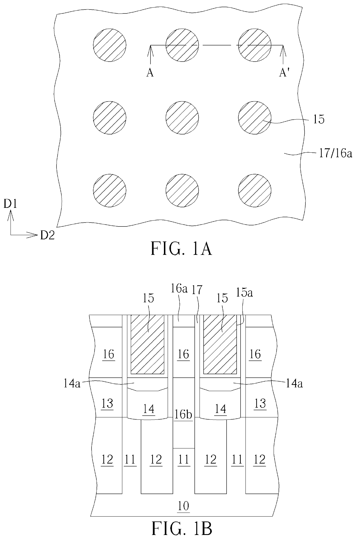
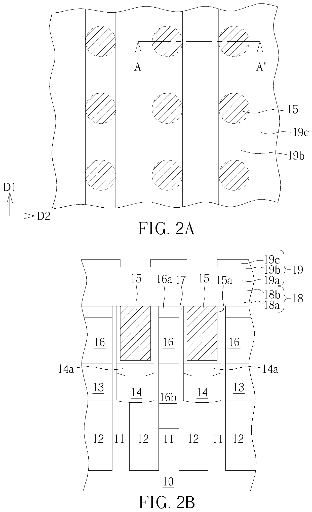
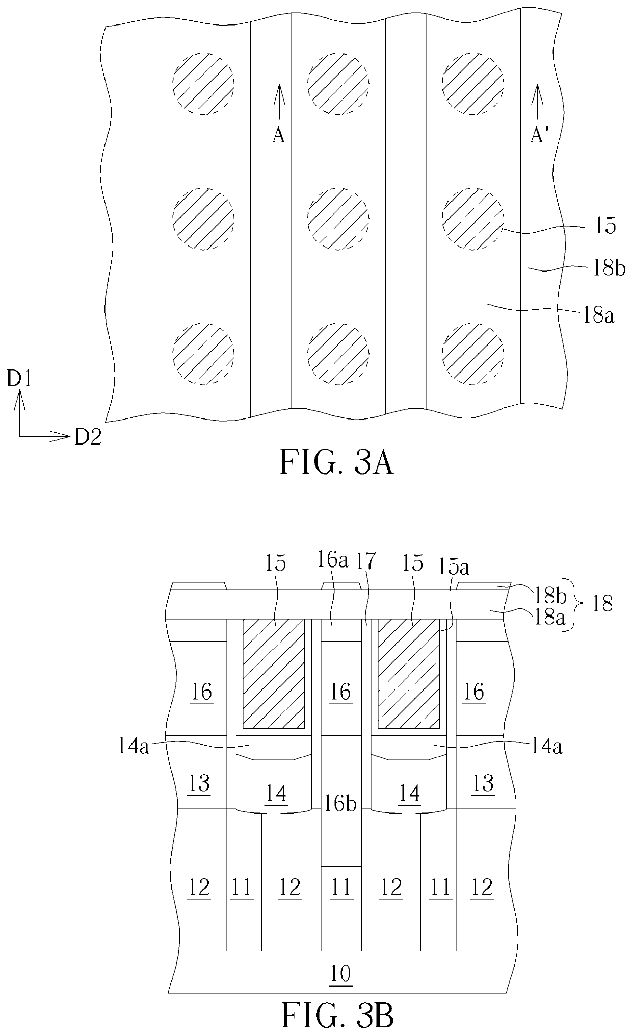
The present invention discloses a semiconductor structure with capacitor landing pad and a method for fabricating a capacitor landing pad. The semiconductor structure with capacitor landing pad includes a substrate having a plurality of contact structures, a first dielectric layer disposed on the substrate and the contact structures, and a plurality of capacitor landing pads, each of the capacitor landing pads being located in the first dielectric layer and electrically connected to the contact structure, wherein the capacitor landing pads presents a shape of a wide top and a narrow bottom and a top surface of the capacitor landing pads have a concave shape.

Description

BACKGROUND OF THE INVENTION[0001]1. Field of the Invention[0002]The present invention relates generally to a method of fabricating a capacitor landing pad. More particularly, the present invention relates to a method for fabricating a landing pad of a storage node in a dynamic random access memory (DRAM) device and the formed structure thereof.[0003]2. Description of the Prior Art[0004]As electronic products develop toward the direction of miniaturization, the design of dynamic random access memory (DRAM) units also moves toward the direction of higher integration and higher density. Since the nature of a DRAM unit with buried gate structures has the advantage of possessing longer carrier channel length within a semiconductor substrate thereby reducing capacitor leakage, it has been gradually used to replace conventional DRAM unit with planar gate structures.[0005]Typically, a DRAM unit with buried gate structure includes a transistor device and a charge storage element to receive e...

Claims


Application Information

Patent Timeline
Patent Type & Authority Patents(United States)
IPC IPC(8): H01L27/108H01L21/8242H01L21/768H01L23/528H01L23/532H10B12/00
CPCH01L27/10885H01L27/10823H01L27/10888H01L27/10891H01L27/10855H01L27/10814H01L27/10876H10B12/03H10B12/30H10B12/315H10B12/0335H10B12/34H10B12/053H10B12/482H10B12/485H10B12/488
Inventor CHANG, FENG-YILEE, FU-CHECHEN, CHIEH-TECHANG, YI-CHING
Owner UNITED MICROELECTRONICS CORP
Learn More