Magnetoresistive magnetic imaging sensor
a magnetic imaging and magneto-resistive technology, applied in the field of magneto-resistive magnetic imaging sensors, can solve the problems of low sensitivity of the magnetic field, large power consumption, low resolution, etc., and achieve the effects of low power consumption, high magnetic field sensitivity, and small siz
- Summary
- Abstract
- Description
- Claims
- Application Information
AI Technical Summary
Benefits of technology
Problems solved by technology
Method used
Image

Examples
embodiment 1
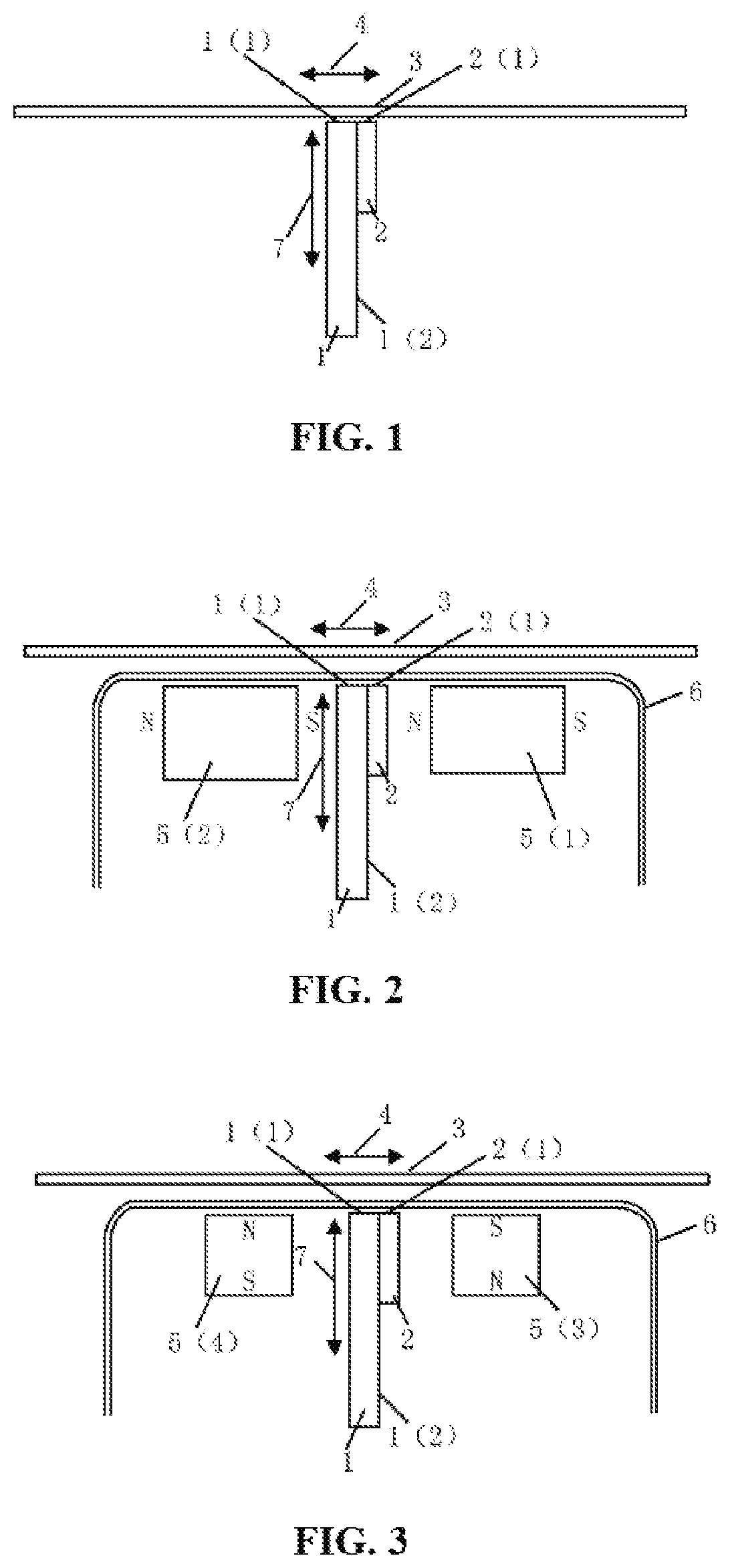
[0050]FIG. 1 is a structural diagram of a lateral detection mode image identification sensor, including a PCB 1 and several magnetoresistive sensor chips 2. A surface having a greater area on the PCB 1 is its front surface 1(2), while a surface adjacent to the front surface 1(2) is its side face 1(1), and the direction of the front surface 1(2) of the PCB 1 is generally referred to as the direction of the PCB 1. Similarly, the magnetoresistive sensor chips 2 also have their front surfaces and side faces 2(1). The several magnetoresistive sensor chips 2 are located on the front surface 1(2) of the PCB 1, and the front surface 1(2) of the PCB 1, where the magnetoresistive sensor chips 2 are located, is perpendicular to a magnetic image detection surface 3. The magnetic image detection surface 3 is a plane where an image to be scanned and detected is located. Each side face 2(1) of the several magnetoresistive sensor chips 2 may be or not be coplanar with the side face 1(1) of the PCB ...
embodiment 2
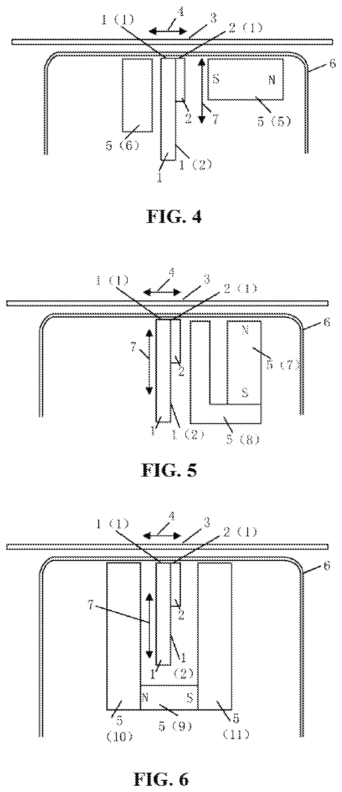
[0051]FIGS. 2-6 are schematic structural diagrams when a lateral detection mode image identification sensor is applied to reading magnetic images formed by soft magnetic materials, and further includes a permanent magnet assembly 5 and a housing 6. The housing 6 covers the outside of the PCB 1 and the several magnetoresistive magnetic sensor chips 2, and the permanent magnet assembly 5 may be wholly located in the housing 6 and may also be partially located in the housing 6 or wholly located outside the housing 6; for ease of description, FIGS. 2-6 only present the situation where the permanent magnet assembly 5 is wholly located in the housing 6. The function of the permanent magnet assembly 5 is to generate a magnetic field to magnetize soft magnetic materials in a magnetic image detection surface 3 made of the soft magnetic materials, to enable the soft magnetic materials to be detected by the several magnetoresistive magnetic sensor chips 2. The function of the housing 6 is to p...
embodiment 3
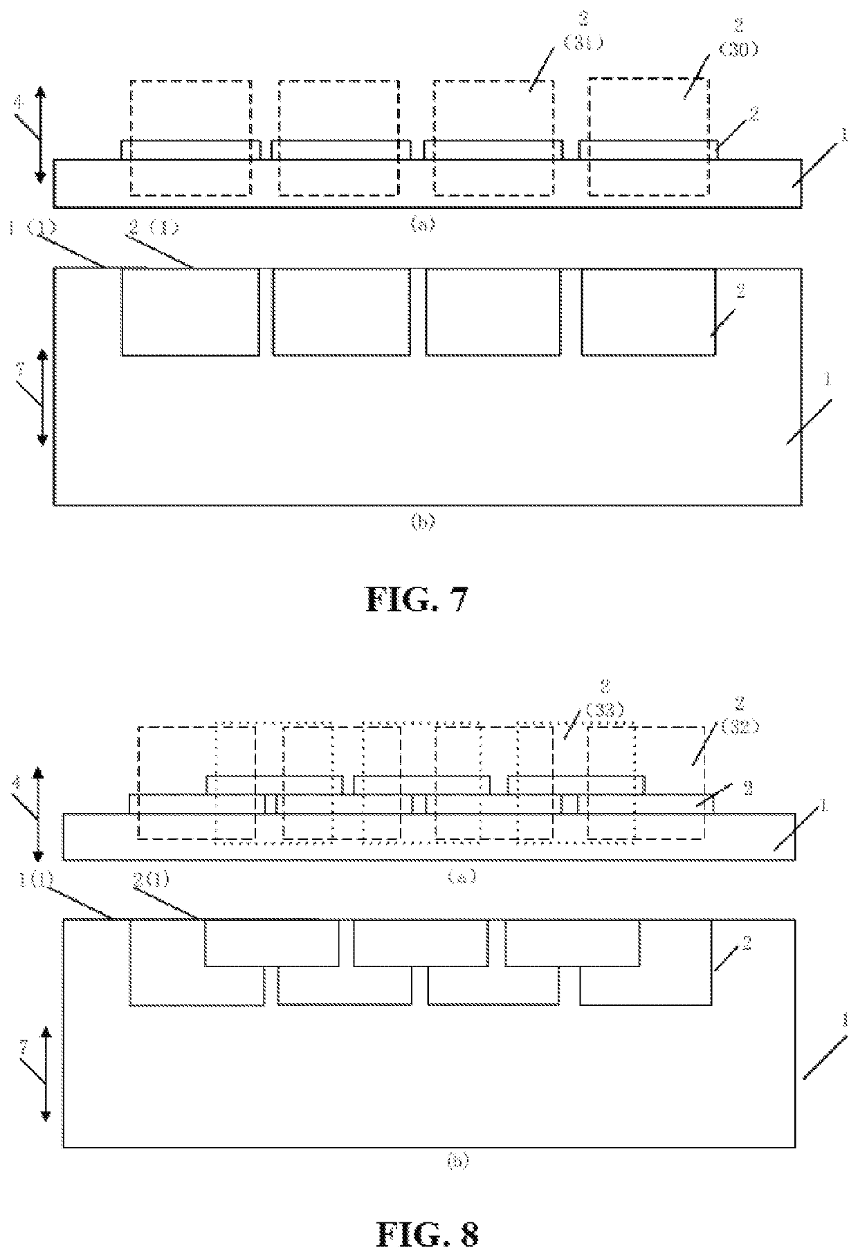
[0057]FIGS. 7-10 are arrangement diagrams of the several magnetoresistive sensor chips 2 in the side mode image identification sensor on the PCB1.
[0058]All the magnetoresistive sensor chips 2 in FIG. 7 are arranged into one row on the PCB 1, FIG. 7(a) is a side view, FIG. 7(b) is a front view, side faces 2(1) of the magnetoresistive sensor chips 2 are arranged sequentially along a side face 1(1) of the PCB 1, and there are gaps among them or the gaps are 0. Such an arrangement method has the following disadvantages: even if in the situation where the gaps are 0, in the presence of packaging materials, scanning detection areas 2(30) and 2(31) formed on the magnetic image detection surface 3 by adjacent magnetoresistive sensor chips 2 along the scanning direction 4 do not intersect with each other, and thus it is impossible to form continuous detection areas in the scanning direction; therefore, there are undetected areas in the detection of the magnetic image.
[0059]In FIGS. 8-10, new...
PUM
| Property | Measurement | Unit |
|---|---|---|
| magnetic | aaaaa | aaaaa |
| magnetization | aaaaa | aaaaa |
| magnetoresistive | aaaaa | aaaaa |
Abstract
Description
Claims
Application Information
 - R&D
- Intellectual Property
- Life Sciences
- Materials
- Tech Scout
- Unparalleled Data Quality
- Higher Quality Content
- 60% Fewer Hallucinations
Browse by: Latest US Patents, China's latest patents, Technical Efficacy Thesaurus, Application Domain, Technology Topic, Popular Technical Reports.
© 2025 PatSnap. All rights reserved.Legal|Privacy policy|Modern Slavery Act Transparency Statement|Sitemap|About US| Contact US: help@patsnap.com