Organic light emitting display panel

a light-emitting display and organic technology, applied in the field of organic light-emitting display panels, can solve the problems of low luminous efficacy of organic electroluminescent display devices, most light beams are lost by total internal reflection, etc., and achieve the effect of efficiently extracting light and improving luminous efficacy

Active Publication Date: 2020-07-21
LG DISPLAY CO LTD
View PDF15 Cites 6 Cited by
  • Summary
  • Abstract
  • Description
  • Claims
  • Application Information

AI Technical Summary

Benefits of technology

[0009]An object of the present invention is to provide an organic light emitting display panel capable of improving luminous efficacy by efficiently extracting light generated in an organic light emitting layer.

Problems solved by technology

All light beams generated in an organic light emitting layer of such an organic electroluminescent display device cannot reach the outside and most of the light beams are lost by total internal reflection.
Since only about ¼ light beams generated in the organic light emitting layer reach the outside, the organic electroluminescent display device has low luminous efficacy.

Method used


Image

  • Organic light emitting display panel
  • Organic light emitting display panel
  • Organic light emitting display panel

Examples


first embodiment

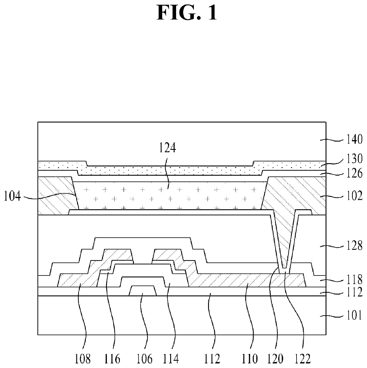
[0028]FIG. 1 is a cross-sectional view illustrating an organic light emitting display panel according to a

[0029]The organic light emitting display panel illustrated in FIG. 1 includes a thin film transistor, a light emitting cell connected to the thin film transistor, a capping layer 130 formed to protect the light emitting cell, and a front sealing layer 140.

[0030]The thin film transistor includes a gate electrode 106, a drain electrode 110 connected to a first electrode 122 of the light emitting cell, a source electrode 108 facing the drain electrode 110, an active layer 114 overlapping the gate electrode 106 while interposing a gate insulating layer 112 therebetween to form a channel between the source electrode 108 and the drain electrode 110, and an ohmic contact layer 116 formed on the active layer 114 except for the channel for ohmic contact with the source electrode 108 and the drain electrode 110.

[0031]An inorganic passivation layer 118 formed of an inorganic insulating mat...

second embodiment

[0049]FIG. 4 is a cross-sectional view illustrating an organic light emitting display panel according to a

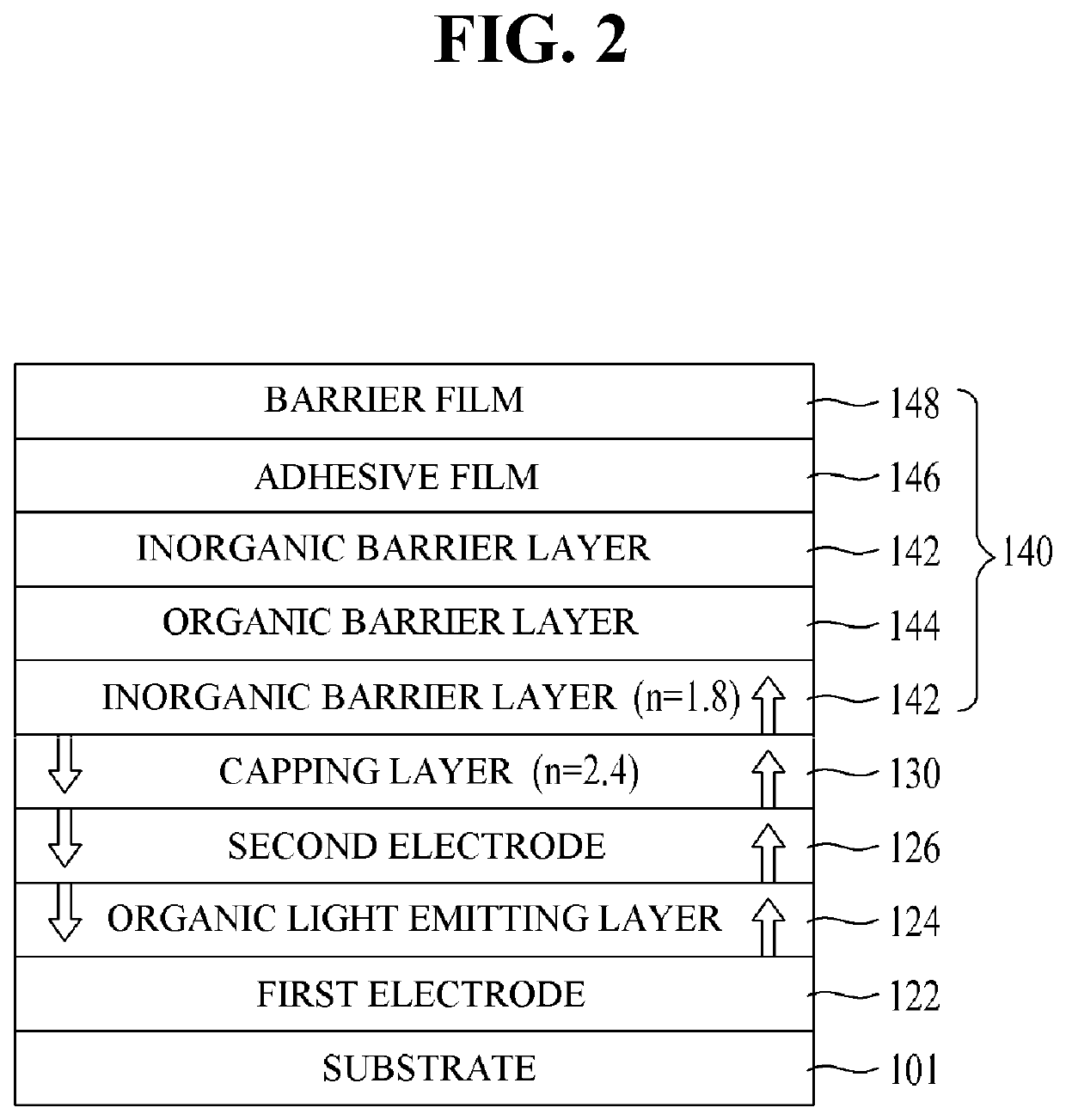
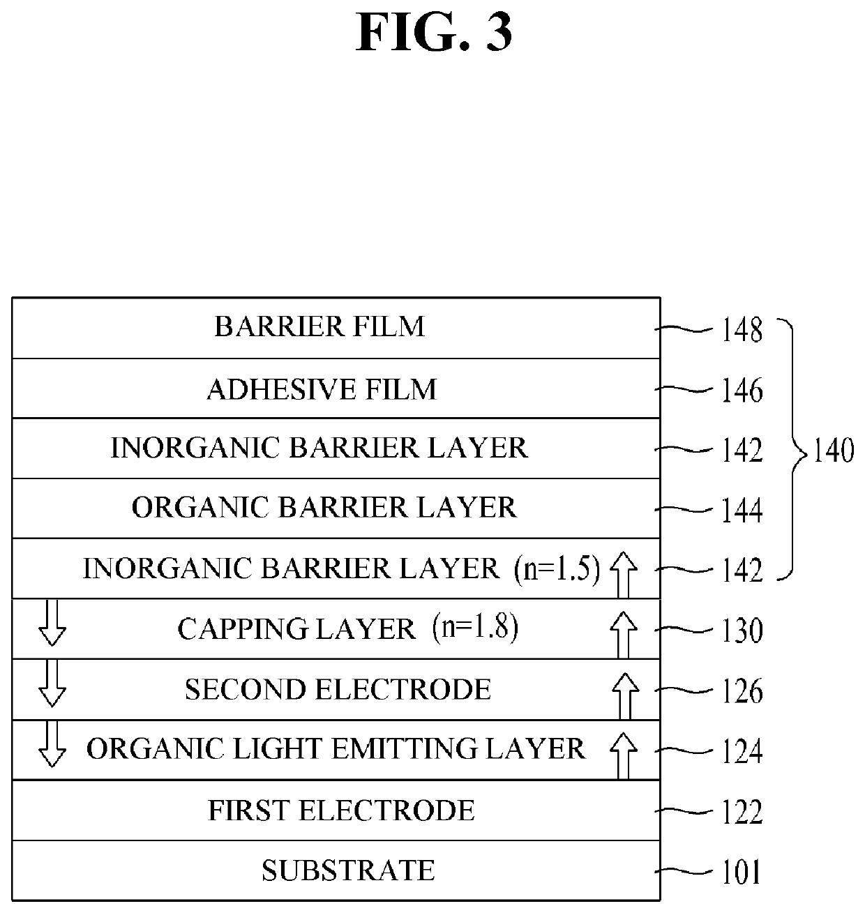
[0050]The organic light emitting display panel illustrated in FIG. 4 has the same elements except that a resonance inducing layer 150 is further formed in comparison with the organic light emitting display panels illustrated in FIGS. 2 and 3 and thus a detailed description thereof will not be given.

[0051]The resonance inducing layer 150 is formed of at least one selected from the group consisting of PA, PI, triamine derivatives, arylene diamine derivatives, CBP, tris(8-hydroxyquinoline)aluminum (Alq3) complexes, SiNx, SiOx, SiON, and LiF between the capping layer 130 and the lowest inorganic barrier layer 142 disposed at the lowest layer of the plurality of thin films contained in the front sealing layer 140. The resonance inducing layer 150 has a lower index of refraction than those of the capping layer 130 and the lowest inorganic barrier layer 142 disposed at both sides of th...


PUM

PropertyMeasurementUnit
thicknessaaaaaaaaaa
thicknessaaaaaaaaaa
thicknessaaaaaaaaaa

Abstract

The organic light emitting display panel includes a first electrode formed on a substrate, an organic light emitting layer formed on the first electrode, a second electrode formed on the organic light emitting layer, a front sealing layer formed on the second electrode, wherein the front sealing layer is formed by alternately laminating an inorganic barrier layer and an organic barrier layer at least once, and at least one capping layer formed between the lowest layer closest to the second electrode among a plurality of thin films of the front sealing layer and the second electrode and having a higher index of refraction than an index of refraction of the lowest layer.

Description

CROSS-REFERENCE TO RELATED APPLICATIONS[0001]This application claims the benefit of Korean Patent Application No. 10-2012-0100317, filed on Sep. 11, 2012 which is hereby incorporated by reference as if fully set forth herein.BACKGROUND[0002]Field of Technology[0003]The embodiments herein relate to an organic light emitting display panel capable of improving luminous efficacy by efficiently extracting light generated in an organic light emitting layer.[0004]Discussion of the Related Art[0005]In recent years, a variety of flat panel display devices having reduced weight and volume, which are drawbacks of cathode ray tubes (CRTs), have been introduced. Examples of flat panel display devices are liquid crystal displays (LCDs), field emission displays (FEDs), plasma display panels (PDPs), and organic electroluminescent displays (ELDs). Among these display devices, an organic electroluminescent display is a self-emitting device operable without a backlight. Owing to excellent characterist...

Claims


Application Information

Patent Timeline
Patent Type & Authority Patents(United States)
IPC IPC(8): H01L51/52
CPCH01L51/52H01L51/5256H01L51/5262H01L2251/5315H01L2251/55H01L2251/558H10K50/8445H10K50/85H10K2102/3026H10K2101/00H10K2102/351H10K50/8426H10K50/80
Inventor CHO, YOUNG-DOCKLEE, KWANG-YEONLEE, HEUI-DONGPARK, EUN-JUNGYUN, HONG-JEMOON, SANG-KYOUNG
Owner LG DISPLAY CO LTD
Why Eureka
Try Eureka