Rewiring method for semiconductor

a technology of semiconductor and rewiring, which is applied in the direction of semiconductor/solid-state device testing/measurement, computer aided design, instruments, etc., can solve the problems of inability to catch up with the tact time (5-10 minutes) of the existing fowlp technique, the difficulty of the photolithography process to achieve a high yield, and the inability to mass production, etc., to achieve the effect of short process cycle, high efficiency and high accuracy

Active Publication Date: 2020-07-28
SHANGHAI MICRO ELECTRONICS EQUIP (GRP) CO LTD
View PDF17 Cites 0 Cited by
  • Summary
  • Abstract
  • Description
  • Claims
  • Application Information

AI Technical Summary

Benefits of technology

[0006]In order to solve the above problems, the present invention proposes a method for rewiring of semiconductor devices, which combines the mask-free and mask-based photolithography approaches and is more time-saving and efficient than techniques only employing mask-free photolithography and is more lithographically accurate than those only utilizing mask-free photolithography.
[0048]Compared to the conventional techniques, the present invention offers the advantages as follows. The present invention provides a method for rewiring of semiconductor devices, in which deviations of electrical connection terminals on a carrier are calculated and corrected by forming rewiring structures on the electrical connection terminals by mask-free photolithography. A wiring layer and / or solder balls is / are then formed on the rewiring structures by processing the carrier in a monolithic manner (without taking into account the deviations) using mask-based photolithography. In this way, the combined use of mask-free photolithography and mask-based photolithography allows for higher efficiency and a shorter process cycle, compared to only using mask-free photolithography.
[0049]The present invention provides another method for rewiring of semiconductor devices, in which deviations of electrical connection terminals on a carrier are calculated and a critical deviation range is determined such that those of the electrical connection terminals whose deviation are below the critical deviation range are processed by mask-based photolithography and those of the electrical connection terminals whose deviation are beyond the critical deviation range are processed by mask-free photolithography. Additionally, for each of the electrical connection terminals whose deviation lies within the critical deviation range, if more than half the surrounding electrical connection terminals are to be processed by one of the photolithography approaches, the electrical connection terminal will also be processed by this photolithography approach. In this way, higher accuracy can be achieved by applying mask-free photolithography to electrical connection terminals requiring relatively great amounts of correction and mask-free photolithography to those requiring small amounts of correction, while similarly allowing higher efficiency and a shorter process cycle by the combination of mask-free photolithography and mask-based photolithography.

Problems solved by technology

This makes it difficult for the photolithography process to achieve a high yield and hence unsuitable for mass production.
Therefore, its throughput in each photolithography cycle is extremely low (each cycle takes 2-3 hours) and cannot catch up with the tact time (5-10 minutes) of the existing FOWLP technique.

Method used


Image

  • Rewiring method for semiconductor
  • Rewiring method for semiconductor
  • Rewiring method for semiconductor

Examples


embodiment 1

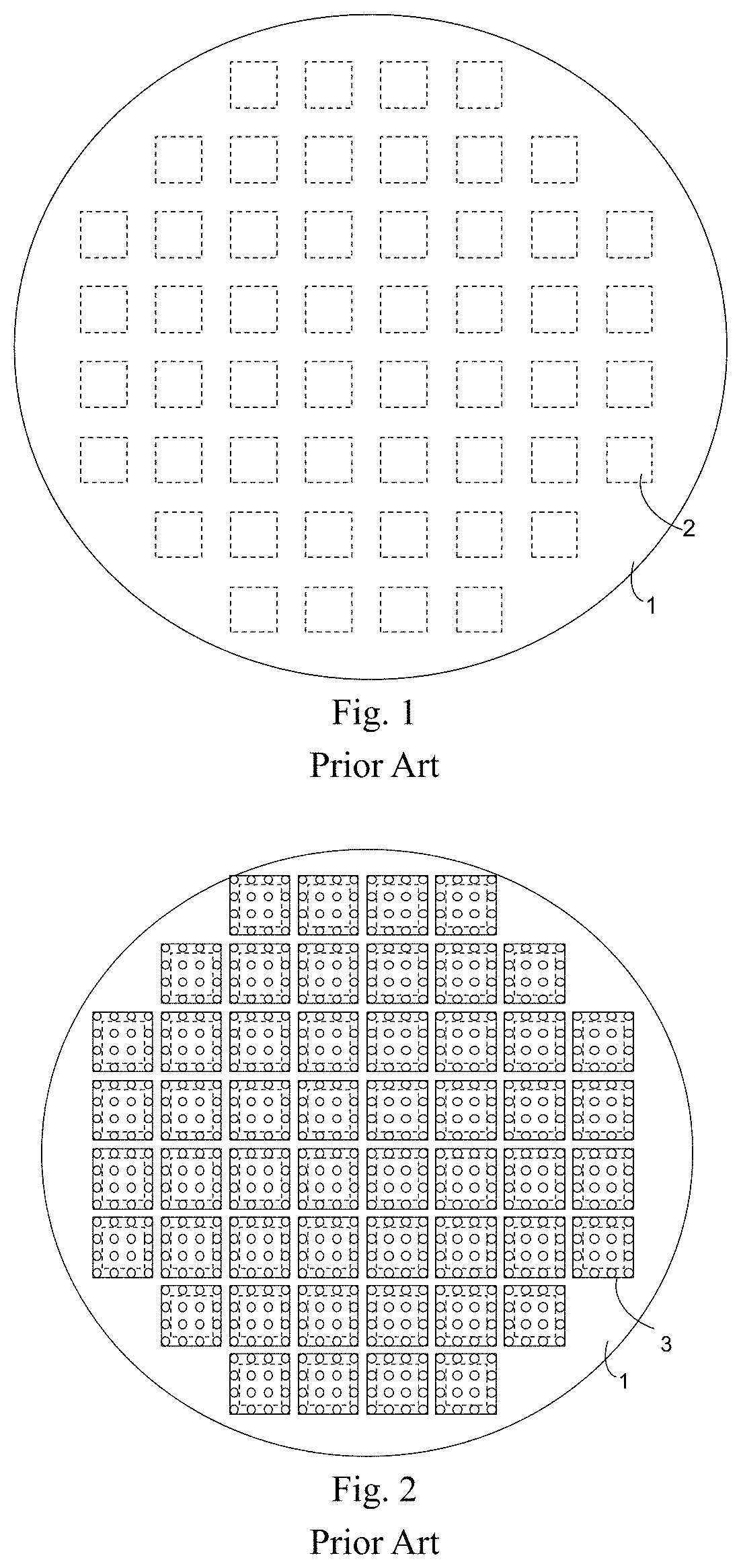
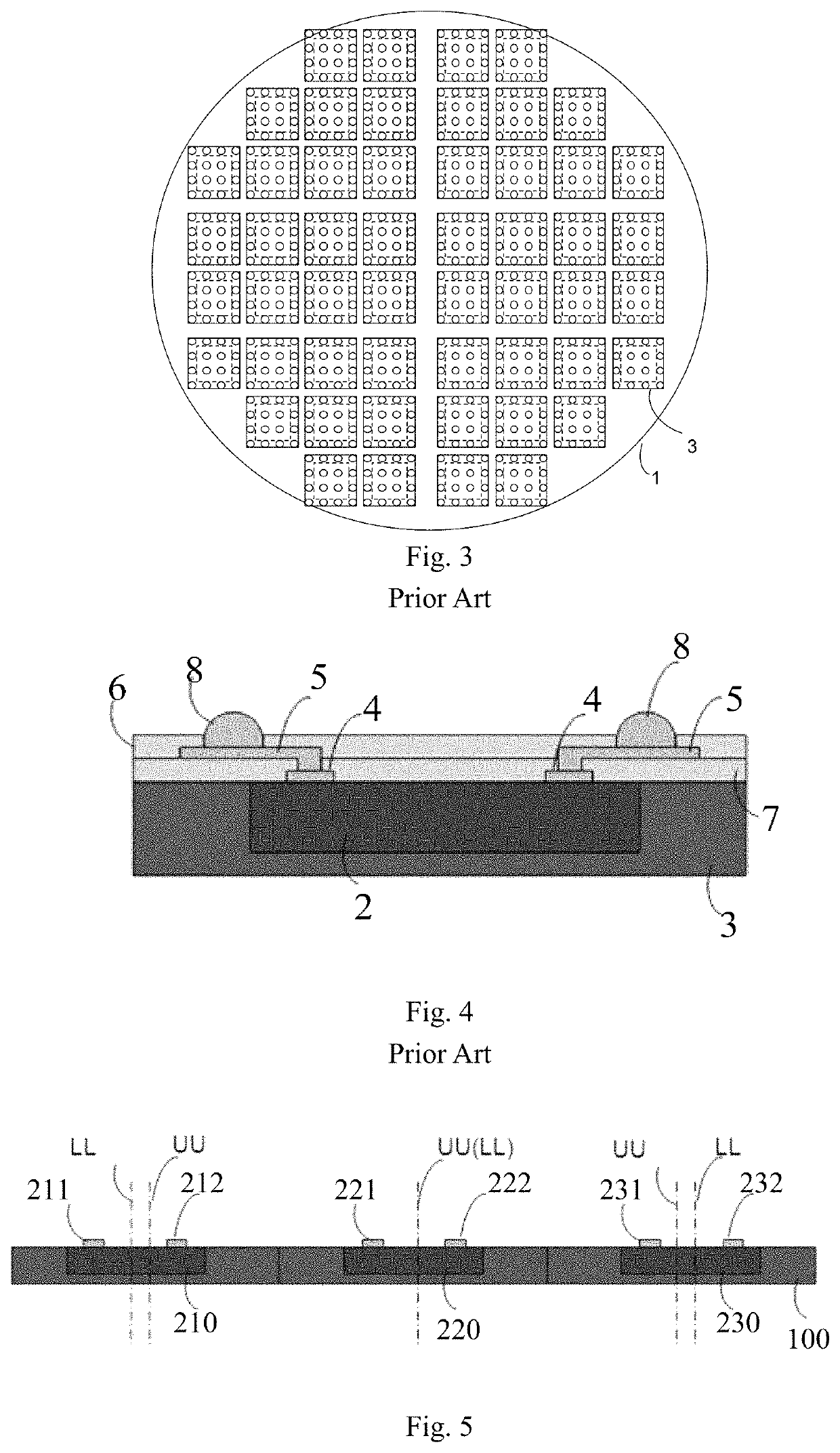
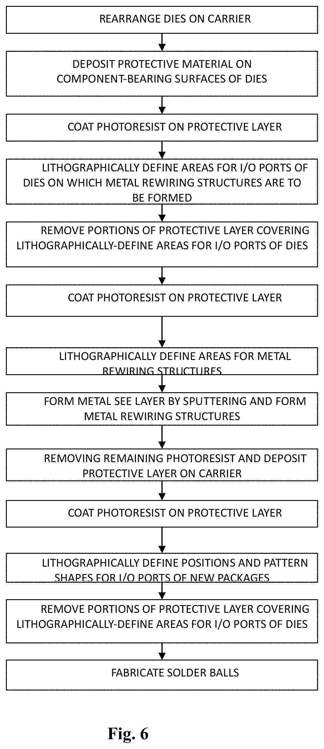
[0081]In a first embodiment of the present invention, there is provided a fan-out wafer-level packaging (FOWLP) method, in which, as shown in FIG. 5, dies are rearranged on a carrier 100. FIG. 5 only illustrates three dies 210, 220, 230 arranged horizontally, each having two I / O ports, i.e., two electrical connection terminals. That is, six electrical connection terminals 211, 212, 221, 222, 231, 232 are shown.

[0082]Here, an X-Y-Z three-dimensional coordinate system is defined with the horizontal direction as the X-axis, the vertical direction as the Z-axis and the direction perpendicular to the X-Z plane as the Y-axis.

[0083]While only three dies 210, 220, 230 are schematically illustrated in FIG. 5, the actual number of the dies arranged on the carrier 100 may be more than three. For each of the dies, standard coordinates of its electrical connection terminals and ball pads are determined in advance based on parameters of a subsequent ball placement process.

[0084]However, as can be...

embodiment 2

[0107]In a second embodiment of the present invention, there is provided a fan-out wafer-level packaging (FOWLP) method, in which when there are a relatively small number of dies rearranged on the carrier 100, positions of the dies, that have been rearranged on the carrier 100, are scanned and mapped, and a critical deviation range is determined based on the actual process conditions. In this embodiment, the critical deviation range is determined as 5-7 μm. For example, only dies with deviations beyond the critical deviation range may be processed by mark-free photolithography, while the remaining ones may be processed by mask-based photolithography. In this manner, a significantly enhanced FOWLP throughput can be achieved.

[0108]Alternatively, dies with deviations beyond the critical deviation range may be processed by mark-free photolithography, and those with deviations below the critical deviation range may be processed by mask-based photolithography. Additionally, each die with ...


PUM

PropertyMeasurementUnit
areasaaaaaaaaaa
sizeaaaaaaaaaa
shapesaaaaaaaaaa

Abstract

A method for rewiring of semiconductor devices is provided, in which deviations of electrical connection terminals (211, 212, 221, 222, 231, 232) on a carrier (100) are calculated and corrected by forming rewiring structures on the electrical connection terminals by mask-free photolithography. A wiring layer and / or solder balls (700) is / are then formed on the rewiring structures by processing the carrier (100) in a monolithic manner using mask-based photolithography. In this way, the combined use of mask-free photolithography and mask-based photolithography allows for higher efficiency and a shorter process cycle, compared to only using mask-free photolithography.

Description

TECHNICAL FIELD[0001]The present invention relates to semiconductor technology and, in particular, to a method for rewiring of semiconductor devices.BACKGROUND[0002]The continuous development of integrated circuit (IC) technology has brought about a trend in electronics toward miniaturization, intelligence, high performance and high reliability. Packaging is critical not only to the performance of individual ICs but to whether the ICs can constitute a compact, low-cost, reliable electronic system. As IC dies continue shrinking in size and increasing in integration, more and more stringent requirements are being placed on IC packaging.[0003]As shown in FIG. 1, fan-out wafer-level packaging (FOWLP) is a packaging technique to rearrange individual dies 2 diced from a wafer on a new carrier 1 for wafer-level packaging. New packages 3 can then be formed on the new carrier 1 using conventional wafer-level packaging techniques (FIG. 2). FIG. 4 depicts a schematic illustration of a single o...

Claims


Application Information

Patent Timeline
Patent Type & Authority Patents(United States)
IPC IPC(8): H01L21/768H01L21/66H01L21/311H01L23/00
CPCH01L21/76897H01L22/20H01L21/76895H01L21/76816H01L21/76877H01L21/31144H01L24/19H01L2224/12105H01L2224/04105H01L21/768H01L2224/32225H01L2224/73267H01L2224/92244H01L2924/15153H01L2224/97H01L2924/37001G06F30/3953G06F30/398H01L2224/83H01L21/0274H01L21/31105H01L24/11
Inventor CHEN, YONGHUITANG, SHIYI
Owner SHANGHAI MICRO ELECTRONICS EQUIP (GRP) CO LTD
Why Eureka
Try Eureka