
Monolithically integrated wavelength converted photonic integrated circuit (PIC) and hybrid fabrication thereof

a photonic integrated circuit and monolithic technology, applied in non-linear optics, instruments, optics, etc., can solve the problem of difficult to realize all of them on a single chip, and achieve the effect of enhancing non-linear susceptibility

Active Publication Date: 2020-12-15
RAYTHEON CO
View PDF18 Cites 5 Cited by
  • Summary
  • Abstract
  • Description
  • Claims
  • Application Information

AI Technical Summary

Benefits of technology

The present invention provides a method for making a photonic circuit that can convert the wavelength of an optical signal. This is achieved by integrating multiple photonic circuits and a wavelength converter into a single material system. The wavelength converter includes a non-linear waveguide and a patterned structure that enhances non-linear susceptibility to generate the desired optical signal at a different wavelength. The patterned structure can also minimize the emission of unwanted harmonics. This invention allows for the creation of more complex and efficient photonic circuits that can be useful in various applications such as optical communication and sensing.

Problems solved by technology

These devices require a variety of different geometries and fabrication techniques making it difficult to realize all of them on a single chip.

Method used


Image

  • Monolithically integrated wavelength converted photonic integrated circuit (PIC) and hybrid fabrication thereof
  • Monolithically integrated wavelength converted photonic integrated circuit (PIC) and hybrid fabrication thereof
  • Monolithically integrated wavelength converted photonic integrated circuit (PIC) and hybrid fabrication thereof

Examples


Embodiment Construction

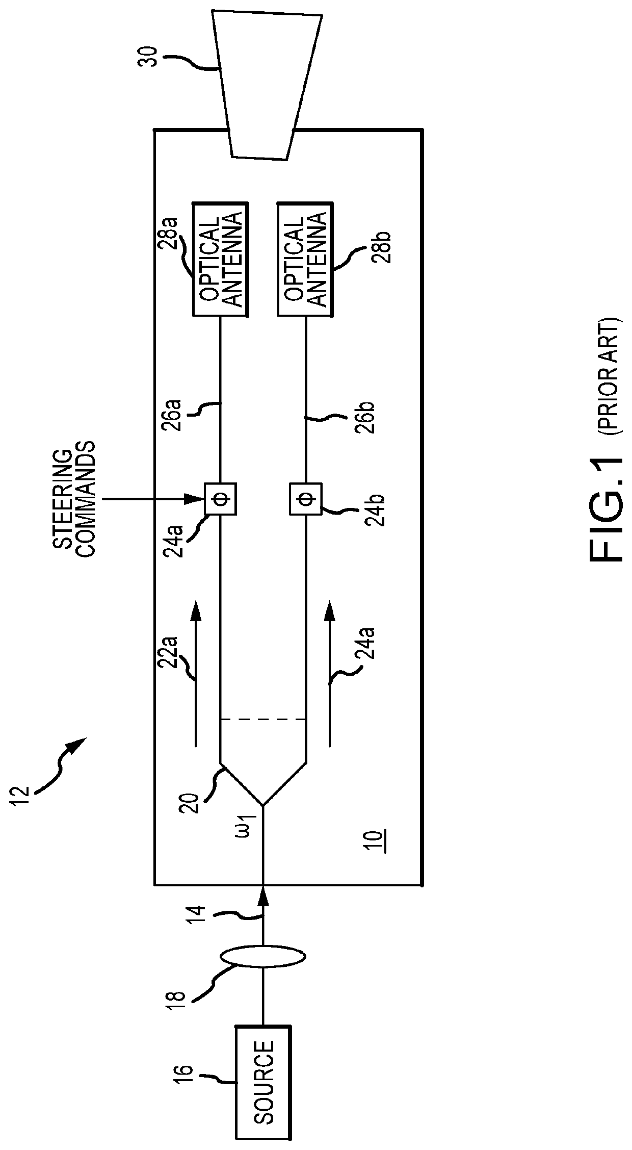
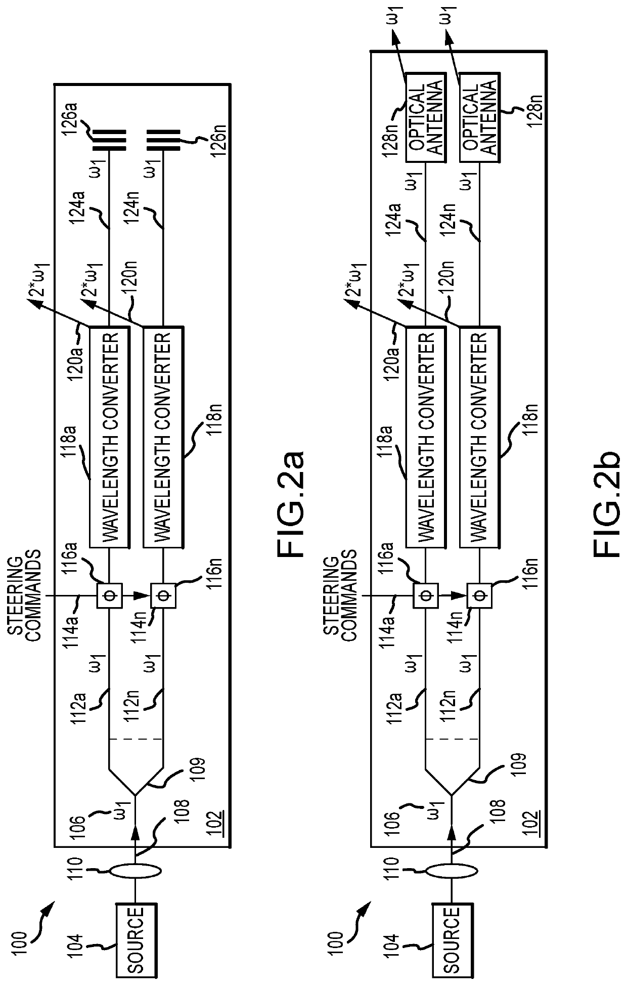
[0027]The present invention describes a monolithically integrated wavelength converted photonic integrated circuit (PIC) to provision optical bands not optimally supported by the underlying PIC. In other words, the PIC may be transmissive at these optical bands but the transmission percentage is too to low photonically process, route and transmit the optical signal without unacceptable losses.

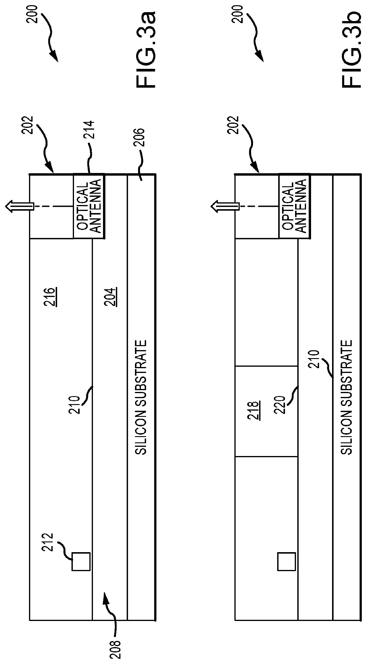
[0028]As previously stated, photonic integrated circuits have been fabricated from a variety of material systems, including electro-optic crystals such as lithium niobate, silica on silicon, SOI, chalcogenides, various polymers, and semiconductor materials which are used to make semiconductor lasers such as GaAs and InP. These materials support different but limited transmission bands. The edges of the transmission band are defined by a specified minimum cut-off transmission e.g. 50%. Within the transmission band, losses due to absorption and reflection are small enough that transmission exceed...


PUM

PropertyMeasurementUnit
wavelengthaaaaaaaaaa

Abstract

A monolithically integrated wavelength converted photonic integrated circuit (PIC) is fabricated by forming a trench in the PIC's insulating layer to expose a portion of an output waveguide that transmits a photonically processed optical signal at frequency ω1. A non-linear waveguide formed of a non-linear material with non-linear susceptibility at frequency ω1 and a transmission bandwidth spanning both ω1 and m*ω1 where m is an integer of at least two is fabricated in direct physical contact with the exposed portion of the output waveguide. A patterned structure is fabricated in or on the non-linear waveguide to enhance non-linear susceptibility to generate an optical signal at frequency m*ω1, which may be emitted directly or coupled to an optical antenna.

Description

BACKGROUND OF THE INVENTIONField of the Invention[0001]This invention relates to photonic integrated circuits (PICs) and more particularly to the monolithic integration of wavelength conversion to provision optical bands not optimally supported by the PIC.Description of the Related Art[0002]A photonic integrated circuit (PIC) is a device that integrates multiple (at least two) photonic functions and as such is similar to an electronic integrated circuit. The major difference between the two is that a photonic integrated circuit provides functions for information signals imposed on optical wavelengths typically in the visible spectrum or near infrared 850 nm-1650 nm.[0003]One of the most commercially utilized material platforms for photonic integrated circuits is indium phosphide (InP), which allows for the integration of various optically active and passive functions on the same chip. Initial examples of photonic integrated circuits were simple 2 section distributed Bragg reflector ...

Claims


Application Information

Patent Timeline
Patent Type & Authority Patents(United States)
IPC IPC(8): G02F1/29G02F1/365G02F1/295G02F1/377
CPCG02F1/292G02F1/377G02F1/365G02F1/2955
Inventor KELLER, SEAN D.UYENO, GERALD P.GLEASON, BENN
Owner RAYTHEON CO
Learn More