
Photoelectric conversion element, imaging device, and electronic apparatus

a technology of photoelectric conversion element and imaging device, which is applied in the direction of color television, television system, radio control device, etc., can solve the problems of deterioration of wavelength selectivity, difficulty in achieving high wavelength selectivity and high response speed, etc., and achieve high color reproducibility, low noise, and high sensitivity.

Active Publication Date: 2020-12-29
SONY SEMICON SOLUTIONS CORP
View PDF31 Cites 0 Cited by
  • Summary
  • Abstract
  • Description
  • Claims
  • Application Information

AI Technical Summary

Benefits of technology

The invention relates to a photoelectric conversion element, an imaging device, and an electronic apparatus which can achieve both high wavelength selectivity and high response speed. This is achieved by providing a photoelectric conversion layer that contains a high-molecular semiconductor material and a low-molecular material with an absorption peak in the wavelength range corresponding to one color in the visible light region. This results in a continuous carrier path in the photoelectric conversion layer, improving sensitivity to light of a specific wavelength range. In summary, the invention allows for improved response speed and wavelength selectivity.

Problems solved by technology

It is, however, difficult to achieve both of high wavelength selectivity and high response speed.
There has been a concern that, when the wavelength selectivity is improved, sufficient response speed is not obtainable, or when the response speed is improved, the wavelength selectivity is deteriorated.

Method used


Image

  • Photoelectric conversion element, imaging device, and electronic apparatus
  • Photoelectric conversion element, imaging device, and electronic apparatus
  • Photoelectric conversion element, imaging device, and electronic apparatus

Examples


modification example (

2. Modification example (example including plurality of organic photoelectric converters)

[0037]2-1. Basic configuration

[0038]2-2. Action and effects

application example

3. Application example

4. Examples

1. EMBODIMENT

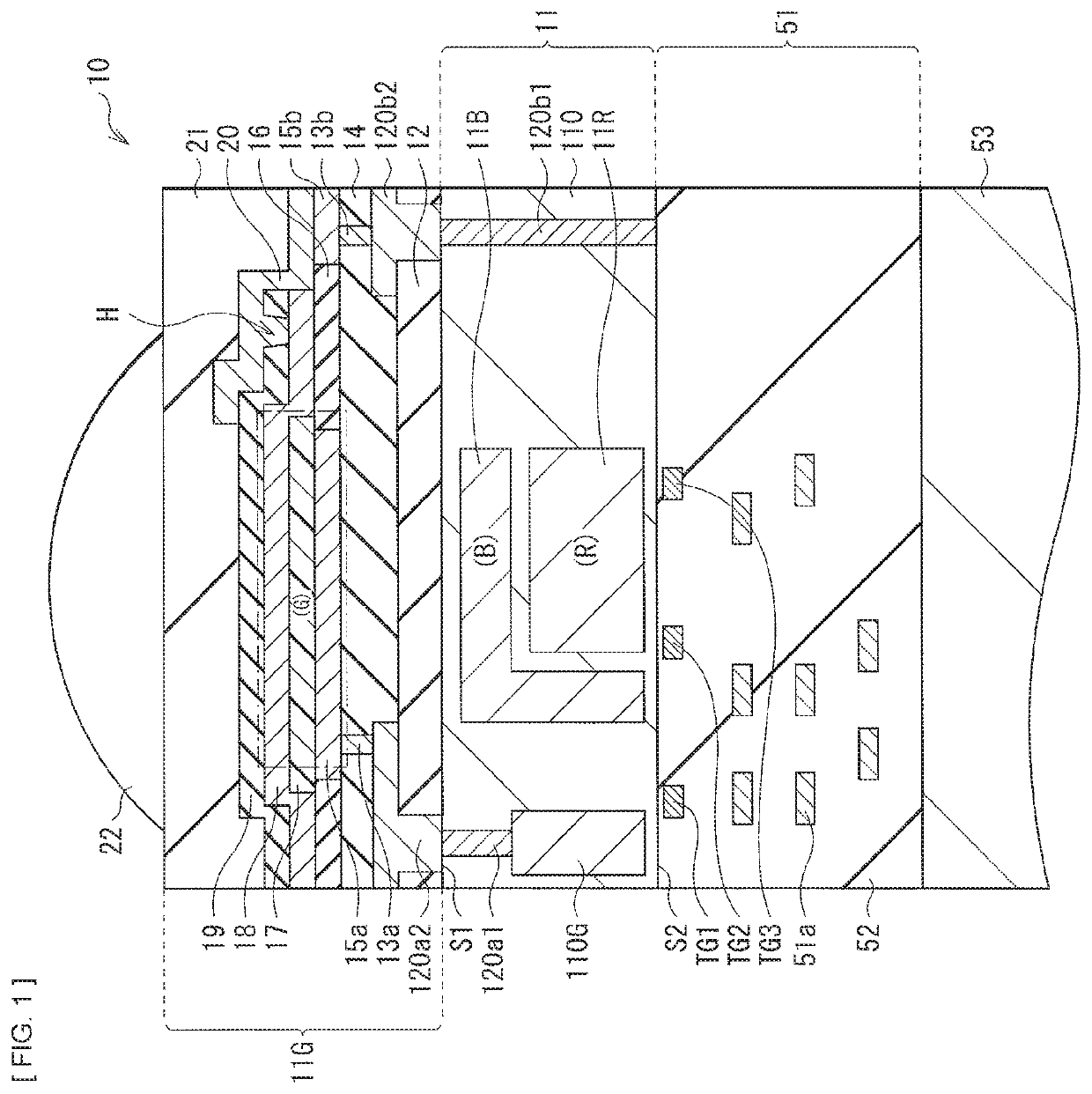
[0039]FIG. 1 illustrates a cross-sectional configuration of a photoelectric conversion element (photoelectric conversion element 10) according to an embodiment of the disclosure. For example, the photoelectric conversion element 10 configures one pixel in an imaging device (described later) such as a CCD image sensor and a CMOS image sensor. The photoelectric conversion element 10 includes pixel transistors (including transfer transistors Tr1 to Tr3 described later) and a multilayer wiring layer (multilayer wiring layer 51) on front surface (surface S2 opposite to light receiving surface) side of a semiconductor substrate 11.

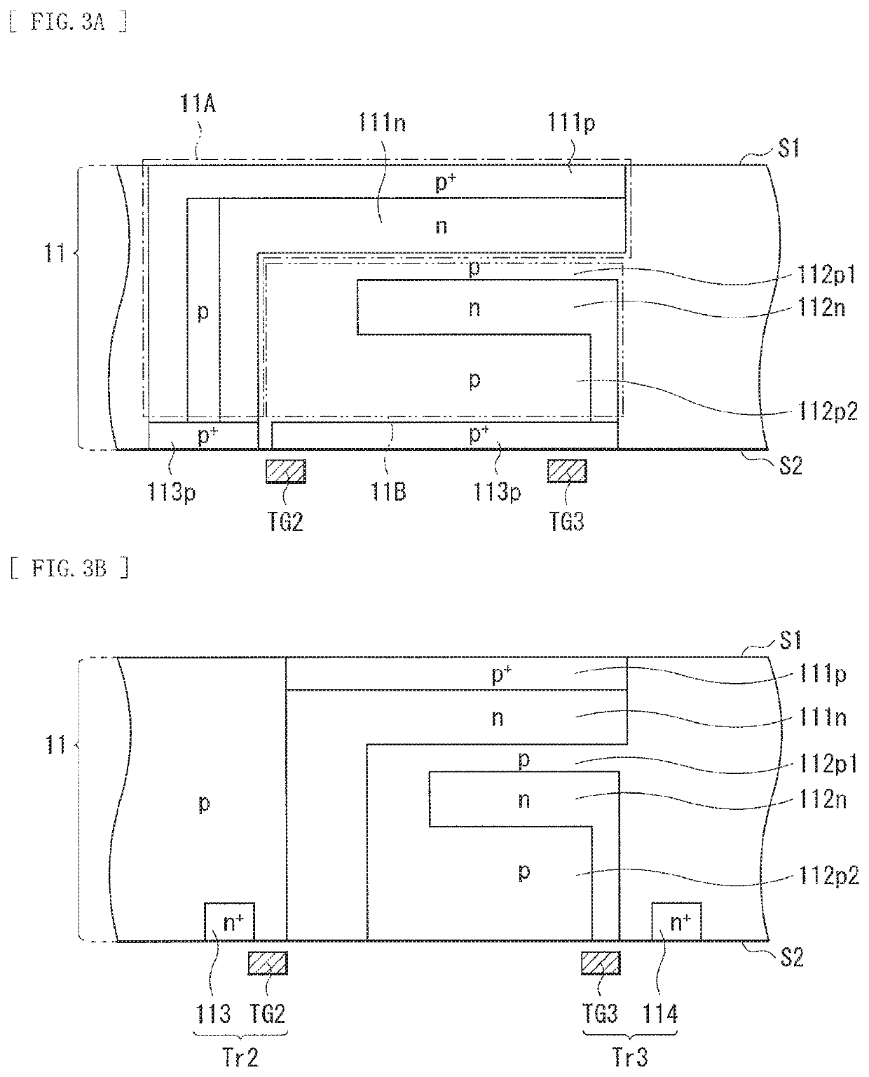
[0040]The photoelectric conversion element 10 according to the present embodiment includes a structure in which one organic photoelectric converter 11G and two inorganic photoelectric converters 11B and 11R that selectively detect light of wavelength ranges different from one another to perform photoelectric conversi...

modification example

2. MODIFICATION EXAMPLE

[0103]FIG. 10 illustrates a cross-sectional configuration of a photoelectric conversion element (photoelectric conversion element 30) according to a modification example of the disclosure. The photoelectric conversion element 30 configures, for example, one pixel (e.g., pixel P in FIG. 11 described later) in an imaging unit (e.g., imaging device 1 in FIG. 11 described later) such as a CCD image sensor and a CMOS image sensor. The photoelectric conversion element 30 includes a red photoelectric converter 30R, a green photoelectric converter 30G, and a blue photoelectric converter 30B in this order on the semiconductor substrate 11 with an insulation layer 42 in between.

[0104]In the photoelectric conversion element 30 according to the present modification example, each photoelectric converter 30R (30G or 30B) includes a photoelectric conversion layer 32R (32G or 31G) between a pair of electrodes, a first electrode 31R (31G or 31B) and a second electrode 33R (33G...


PUM

PropertyMeasurementUnit
absorption coefficientaaaaaaaaaa
first wavelength rangeaaaaaaaaaa
wavelength rangeaaaaaaaaaa

Abstract

A photoelectric conversion element according to one embodiment of the disclosure includes: a first electrode and a second electrode that are oppositely disposed; and a photoelectric conversion layer that is provided between the first electrode and the second electrode, and includes a high-molecular semiconductor material and a low-molecular material. The high-molecular semiconductor material has an absorption coefficient in a visible light region of 50000 cm−1 or less. The low-molecular material includes an absorption peak in a wavelength range corresponding to one color in the visible light region.

Description

CROSS REFERENCE TO RELATED APPLICATIONS[0001]This application is a U.S. National Phase of International Patent Application No. PCT / JP2016 / 073416 filed on Aug. 9, 2016, which claims priority benefit of Japanese Patent Application No. JP 2015-168322 filed in the Japan Patent Office on Aug. 27, 2015. Each of the above-referenced applications is hereby incorporated herein by reference in its entirety.TECHNICAL FIELD[0002]The disclosure relates to, for example, a photoelectric conversion element using an organic semiconductor, and to an imaging device and an electronic apparatus each including the photoelectric conversion element.BACKGROUND ART[0003]In recent years, reduction of a pixel size is progressing in a solid-state imaging unit such as a CCD (Charge Coupled Device) image sensor and a CMOS (Complementary Metal Oxide Semiconductor) image sensor. Therefore, the number of photons entering a unit pixel is decreased, which deteriorates sensitivity and an S / N ratio. In addition, in a ca...

Claims


Application Information

Patent Timeline
Patent Type & Authority Patents(United States)
IPC IPC(8): H01L27/30H01L27/146H01L27/28H01L51/00H04N5/369H01L51/42H01L51/44H10K99/00
CPCH01L51/0047H01L51/0072H01L51/0068H01L51/442H01L51/42H01L27/14647H01L51/006H01L51/008H01L27/307H01L27/286H01L27/14665H01L51/4253H04N5/369H01L51/0039H01L27/1461H01L51/0058Y02E10/549H10K19/20H10K39/32H10K85/115H10K85/113H10K85/111H10K85/215H10K85/633H10K85/655H10K85/322H10K85/6572H10K30/00H10K30/30H10K30/82H10K85/626
Inventor SAITO, YOSUKEOBANA, YOSHIAKIMATSUZAWA, NOBUYUKI
Owner SONY SEMICON SOLUTIONS CORP
Learn More