Ceramic foam for helium light-up suppression

a technology of helium light-up and foam, which is applied in the direction of electrical equipment, basic electric elements, electric discharge tubes, etc., can solve the problems of electrical discharge, ignition damage to esc and/or other chamber components, etc., to reduce the overall kinetic energy of gas, reduce the probability, and reduce the mean free path of thermal conductance gas

Active Publication Date: 2021-01-19
LAM RES CORP
View PDF20 Cites 2 Cited by
  • Summary
  • Abstract
  • Description
  • Claims
  • Application Information

AI Technical Summary

Benefits of technology

[0006]An ESC in a chamber of a semiconductor manufacturing apparatus is presented for eliminating cooling-gas light-up. One wafer support includes a baseplate connected to a radiofrequency power source, a dielectric block, gas supply channels for cooling the wafer bottom, and ceramic foam plugs inserted within gas delivery channels where gas light-up would otherwise occur. The dielectric block is situated above the baseplate and supports the wafer during operation of the chamber. As used herein, gas delivery channels may be referred to as plug channels for their ability to hold in place the ceramic foam plugs. The ceramic foam plugs are formed to have pores of such a range of sizes that reduce the mean free path of the thermal conductance gas while flowing through the gas delivery channel. In so doing, the ceramic foam plugs reduce the likelihood that any given gas molecule is able to be accelerated in any given direction by the electric field for a relatively long distance. As a result, the overall kinetic energy of the gas is reduced and so is the likelihood of light-up events.

Problems solved by technology

The high voltage applied across the ceramic may cause electrical discharge (i.e., arcing) between the wafer and the baseplate, and may cause ignition of the thermal conductance gas (e.g., He, or other chemistry) in the gas supplying holes.
Arcing in the ESC may cause damage to the ESC and / or damage to other chamber components.
Further, such arcing may in some cases cause interruption of the manufacturing process.
Sometimes the destruction of the ESC is fast, catastrophic, and easily detected, but other times there is a gradual deterioration that may unknowingly affect multiple wafers, and the damage to the wafers may only be detectable at later steps of the manufacturing process.

Method used


Image

  • Ceramic foam for helium light-up suppression
  • Ceramic foam for helium light-up suppression
  • Ceramic foam for helium light-up suppression

Examples


Embodiment Construction

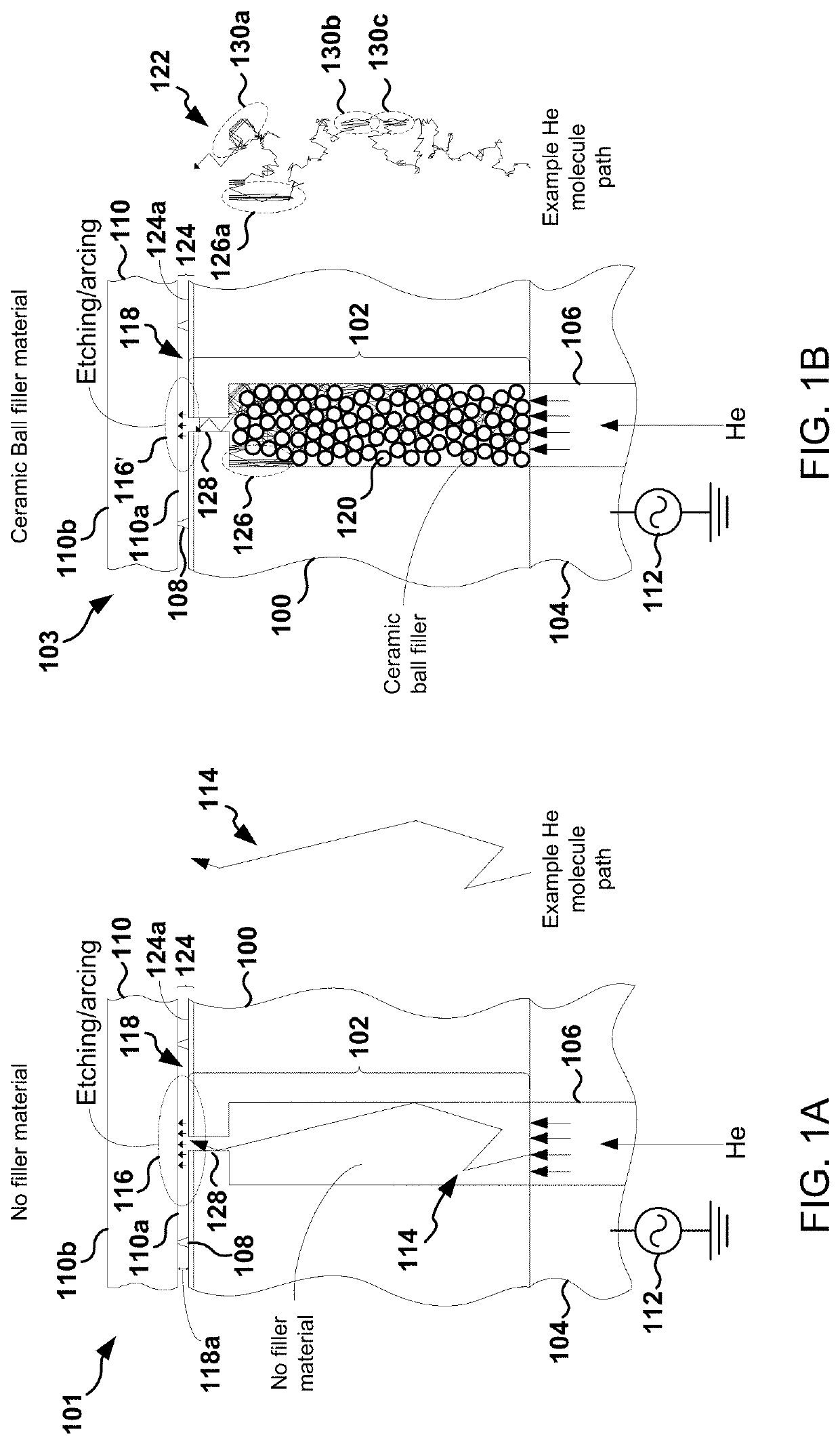
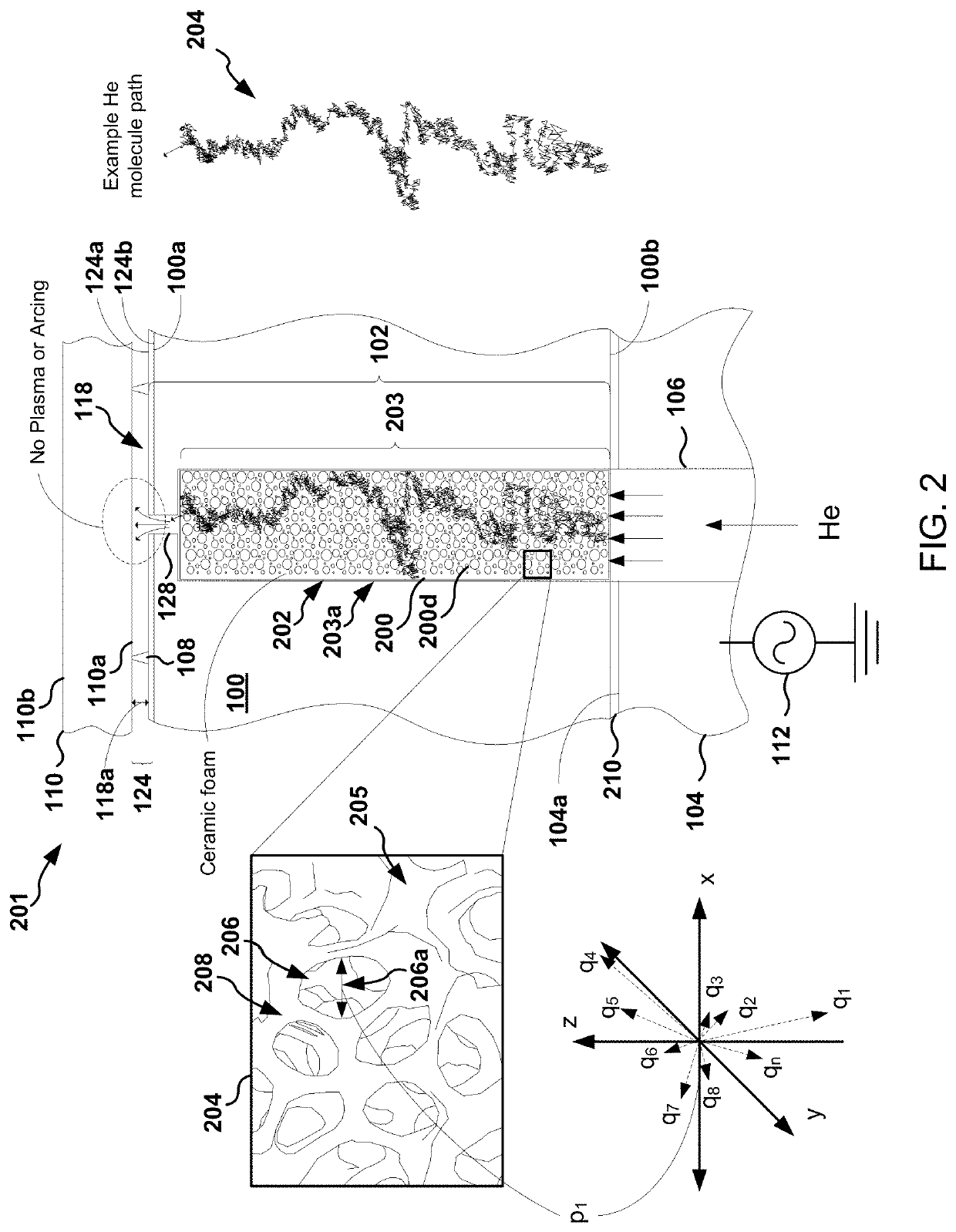
[0024]The following embodiments describe systems, methods, and devices for eliminating thermal conductance gas light-up within an ESC. Embodiments presented described solutions for eliminating arcing in the ESC, and for solving the potential problem of gas (e.g., He) light-up, by forming and using ceramic foam plugs inside gas delivery channels where arcing and lighting-up have been found to occur within the ESC.

[0025]ESCs used in plasma reactors distribute helium (He) as a thermal transport material between the chuck surface and backside of a clamped wafer. Helium is distributed through delivery holes in a dielectric upper portion of the ESC. At high, or even modest bias voltages, helium gas in the delivery holes can break down (e.g., ionize) and become plasma. As a result, etching of the backside of the wafer may occur. In certain circumstances, arcing between the baseplate of the ESC and the wafer may also occur. Inadvertent etching of the backside of the wafer produces visible m...


PUM

PropertyMeasurementUnit
porosityaaaaaaaaaa
pore sizesaaaaaaaaaa
porosityaaaaaaaaaa

Abstract

A substrate support assembly for use in an electrostatic chuck (ESC) in a chamber of a semiconductor manufacturing apparatus is presented for eliminating thermal conductance gas light-up. In one embodiment, the substrate support assembly includes a dielectric block having an upper surface for interfacing with a substrate support surface and a lower surface configured for interfacing with a baseplate. The assembly further includes a plurality of plug channels for introducing gas through the dielectric block to a temperature conduction region between the substrate support surface and a lower surface of the substrate. Each of plug channels contains a ceramic foam plug having a body and a pre-formed pore matrix that is integrally distributed through the body for reducing the mean free path of the gas.

Description

BACKGROUND1. Field of the Invention[0001]The present disclosure relates to systems and methods for improving the design of an electrostatic chuck (ESC), and more particularly, for eliminating light-up of thermal conductance gas within the ESC.2. Description of the Related Art[0002]Some new semiconductor manufacturing processes utilize very high radio frequency (RF) power to generate plasma. The high RF power increases the RF currents and total voltages applied to the ESC, also referred to herein as chuck or wafer susceptor, when compared to previous solutions with lower RF power levels.[0003]In addition, some new plasma etch processes require significantly lower RF frequencies (e.g., 2 MHz or lower) than previously utilized. The lower RF frequencies cause an increase in the RF voltage applied across the ESC ceramic. The high voltage applied across the ceramic may cause electrical discharge (i.e., arcing) between the wafer and the baseplate, and may cause ignition of the thermal cond...

Claims


Application Information

Patent Timeline
Patent Type & Authority Patents(United States)
IPC IPC(8): H01L21/683H01L21/67H01J37/32
CPCH01L21/6833H01L21/67103H01J37/3244H01J37/32082H01J37/32568H01J37/32715H01L21/68785H01L21/67109H01L21/6831H01L21/68757
Inventor PILGRIM, GREGORY A.
Owner LAM RES CORP
Why Eureka
Try Eureka