

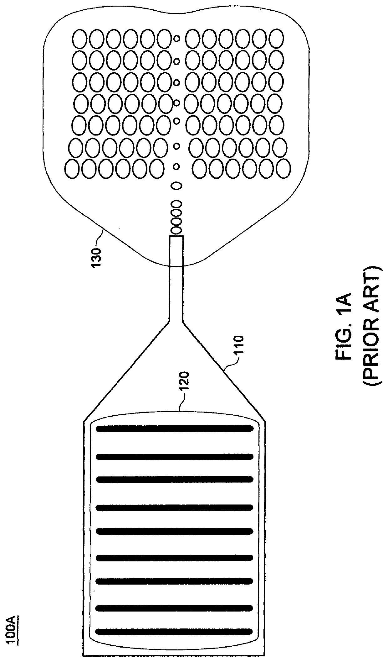
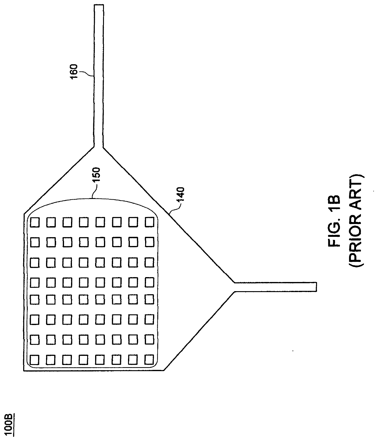
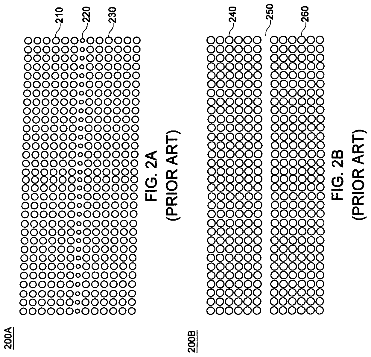
Integrated thermal sensor comprising a photonic crystal waveguide
a thermal sensor and photonic crystal waveguide technology, applied in the field of integrated thermal sensors, can solve the problems of increasing the ratio of electrical conductivity to thermal conductivity, not disclosing a thermal micro-platform supported by nanowires, and not disclosing a pcw-based sensor, so as to reduce the mean free path of thermal energy transport, reduce the electrical conductivity of nanowires, and reduce the effect of the free path
- Summary
- Abstract
- Description
- Claims
- Application Information
AI Technical Summary
Benefits of technology
Problems solved by technology
Method used
Image

Examples
Embodiment Construction
[0098]Definitions: The following terms are explicitly defined for use in this disclosure and the appended claims:
[0099]“photonic” means electromagnetic energy having wavelengths ranging from visible to millimeters.
[0100]“analyte” means a gas, vapor, particulates affecting the photonic carrier signal detected from a photonic crystal waveguide sensor (PCWS) for the purpose of identification, monitoring or calibration.
[0101]“photonic element” or “photonic structure” means a structure providing variously a source, interface, coupling, focusing, guiding, switching, termination and sensing for a photonic carrier signal.
[0102]“phononic structure” means a structure for sourcing, interfacing, coupling, scattering, and resonating thermal phonons.
[0103]“light emitting platform” or “LEP” means a photonic element comprising a thermal micro-platform heated to a temperature providing a photonic source (PS).
[0104]“thermoelectric device” means a device for converting a temperature differential into ...
PUM
| Property | Measurement | Unit |
|---|---|---|
| wavelengths | aaaaa | aaaaa |
| wavelengths | aaaaa | aaaaa |
| wavelength range | aaaaa | aaaaa |
Abstract
Description
Claims
Application Information